
Compact Muon Solenoid
LHC, CERN
| CMS-TRK-20-002 ; CERN-EP-2025-036 | ||
| Operation and performance of the CMS silicon strip tracker with proton-proton collisions at the CERN LHC | ||
| CMS Collaboration | ||
| 20 June 2025 | ||
| JINST 20 (2025) P08027 | ||
| Abstract: Salient aspects of the commissioning, calibration, and performance of the CMS silicon strip tracker are discussed, drawing on experience during operation with proton-proton collisions delivered by the CERN LHC. The data were obtained with a variety of luminosities. The operating temperature of the strip tracker was changed several times during this period and results are shown as a function of temperature in several cases. Details of the system performance are presented, including occupancy, signal-to-noise ratio, Lorentz angle, and single-hit spatial resolution. Saturation effects in the APV25 readout chip preamplifier observed during early Run 2 are presented, showing the effect on various observables and the subsequent remedy. Studies of radiation effects on the strip tracker are presented both for the optical readout links and the silicon sensors. The observed effects are compared to simulation, where available, and they generally agree well with expectations. | ||
| Links: e-print arXiv:2506.17195 [hep-ex] (PDF) ; CDS record ; inSPIRE record ; CADI line (restricted) ; | ||
| Figures | |
png pdf |
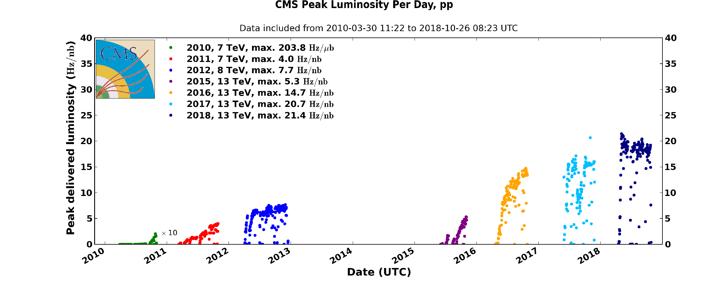
Figure 1:
Peak luminosity delivered to CMS during stable pp collisions for 2010--2012 and 2015--2018, as a function of time [10]. The luminosity for the year 2010 is multiplied by a factor of 10. |
png pdf |
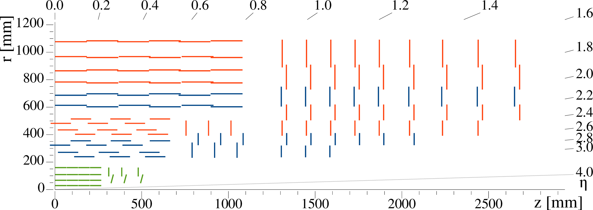
Figure 2:
An $ r-z $ view of one quarter of the CMS silicon strip tracker. Layers with stereo modules (details are given in the main text) are drawn as blue lines, layers with single modules as red lines. The Phase-1 pixel detector, installed in 2017, is shown in green. |
png pdf |
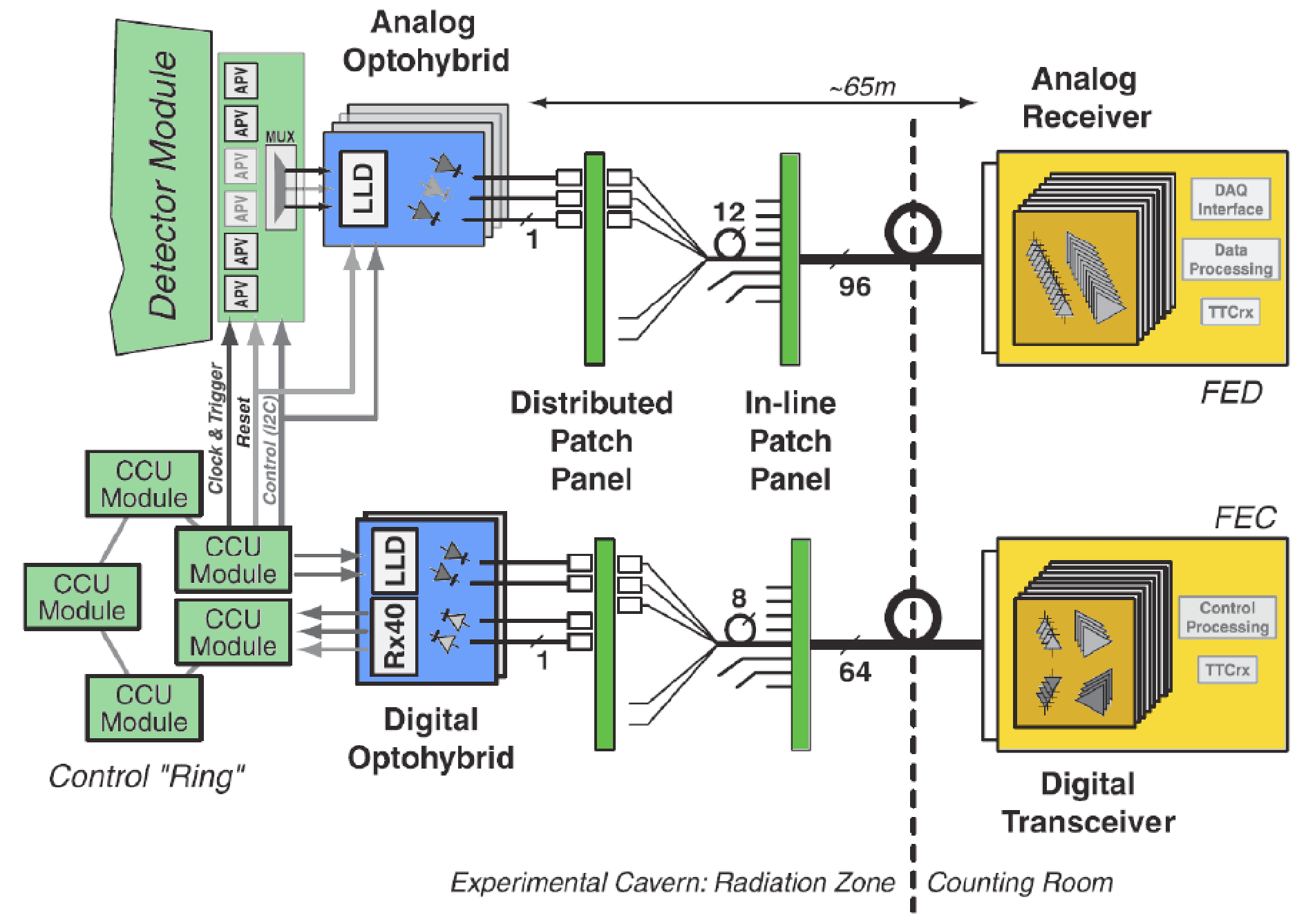
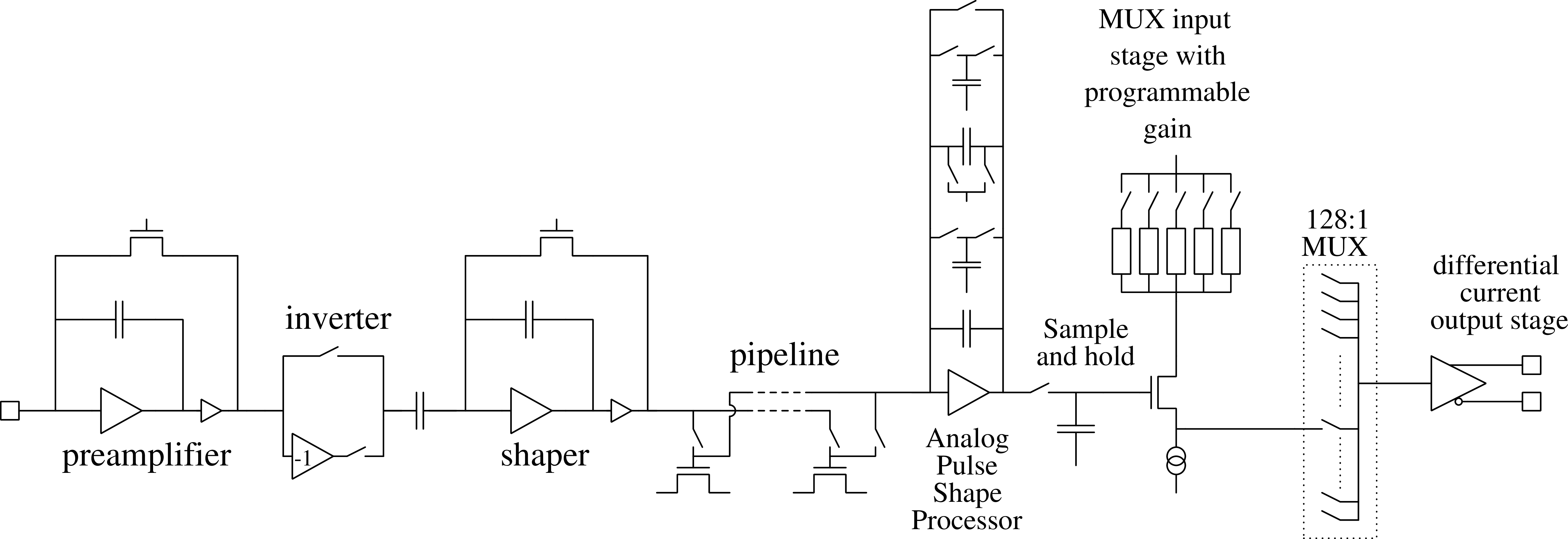
Figure 3:
Overview of the control and readout scheme of the SST. |

png pdf jpg |
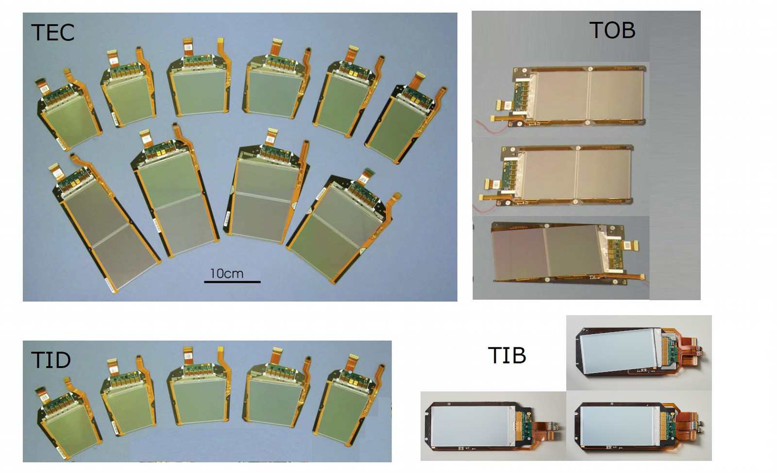
Figure 4:
Module types of the SST. |
png pdf |
Figure 5:
Functional schematic of a single channel of the APV25 chip. |
png pdf |
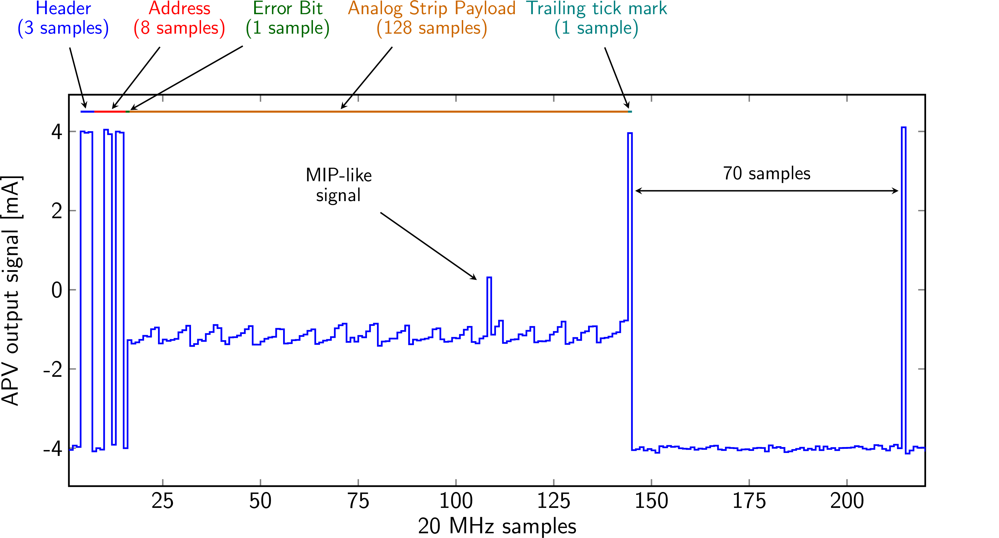
Figure 6:
Example of an APV25 chip output signal. A data frame consists of a 3-bit start-of-frame marker, an 8-bit pipeline address, an error bit, the 128 strip analog payload, and the trailing tick mark. In the absence of a level-1 trigger accept signal, the APV25 chip issues tick mark synchronization pulses every 70 clock cycles. |
png pdf |
Figure 7:
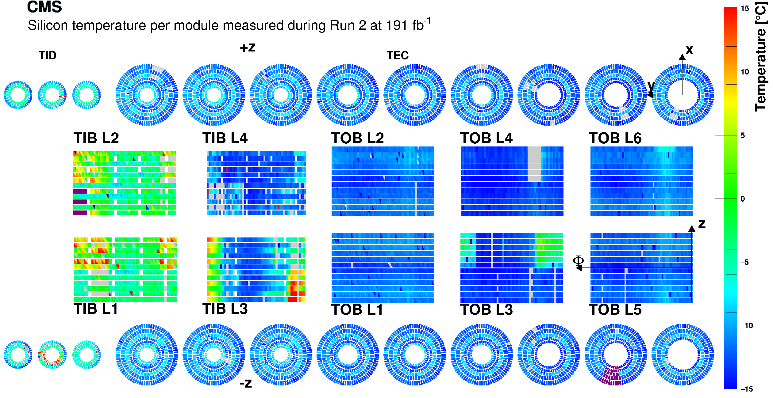
Tracker map where each silicon module is represented by a rectangle in the barrel and a trapezoid in the endcap; in stereo modules each submodule constitutes one half of this area. In the TID and TEC the disks are shown with the distance from the interaction point increasing from left to right. The color scale represents the silicon sensor temperature measured by DCUs after 191 fb$ ^{-1} $ of integrated luminosity at a cooling plant set point of $ -20^\circ $C. Modules in gray are excluded from the data acquisition. The large gray regions in TIB layers 1, 2 and TOB layer 4 are nonfunctioning control rings. The large purple regions in TIB layer 2 and TEC-disk 8 are detector parts that are functional in the data acquisition, but have problems in the readout of slow control data via the DCUs. |
png pdf |
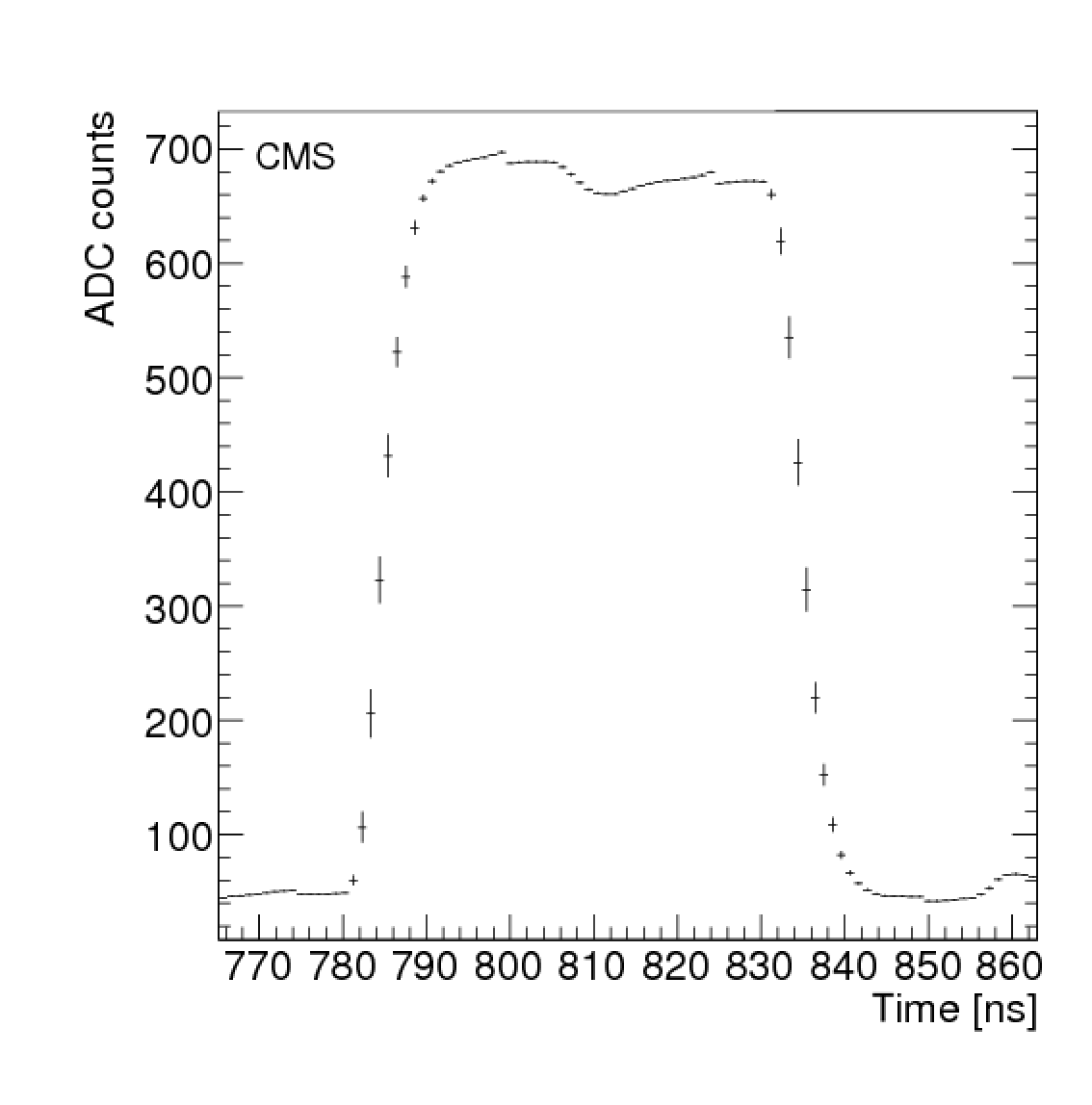
Figure 8:
High-resolution time domain capture of the tick marks from two APV25 chips (1 laser) from one module. The signals from the two APV25 chips are time multiplexed. The tick-height corresponds to an amplitude of about 800 mV. |
png pdf |
Figure 9:
Illustration of pulse modulation by the LLD (left) and visualization of the bias setting scan during the optical link setup run for one LLD gain setting (right). |
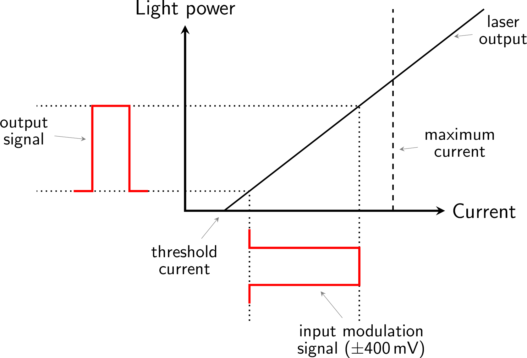
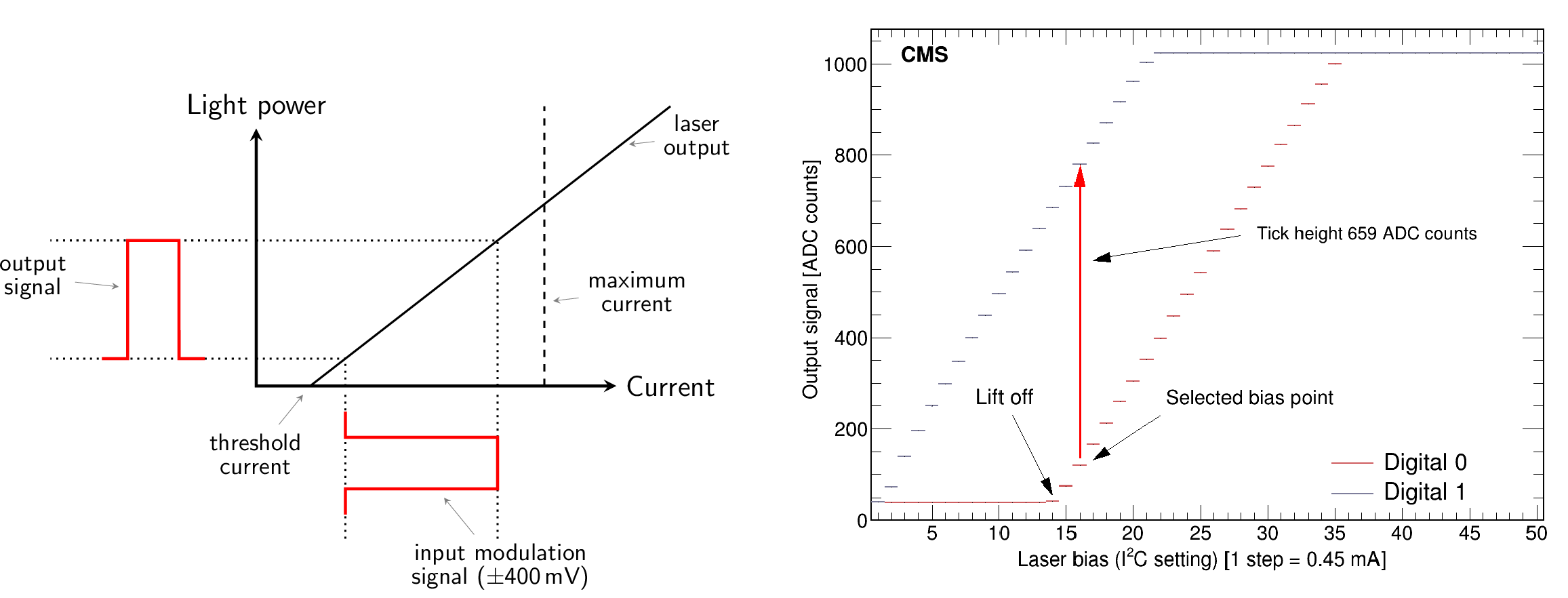
png pdf |
Figure 9-a:
Illustration of pulse modulation by the LLD (left) and visualization of the bias setting scan during the optical link setup run for one LLD gain setting (right). |
png |
Figure 9-b:
Illustration of pulse modulation by the LLD (left) and visualization of the bias setting scan during the optical link setup run for one LLD gain setting (right). |
png pdf |
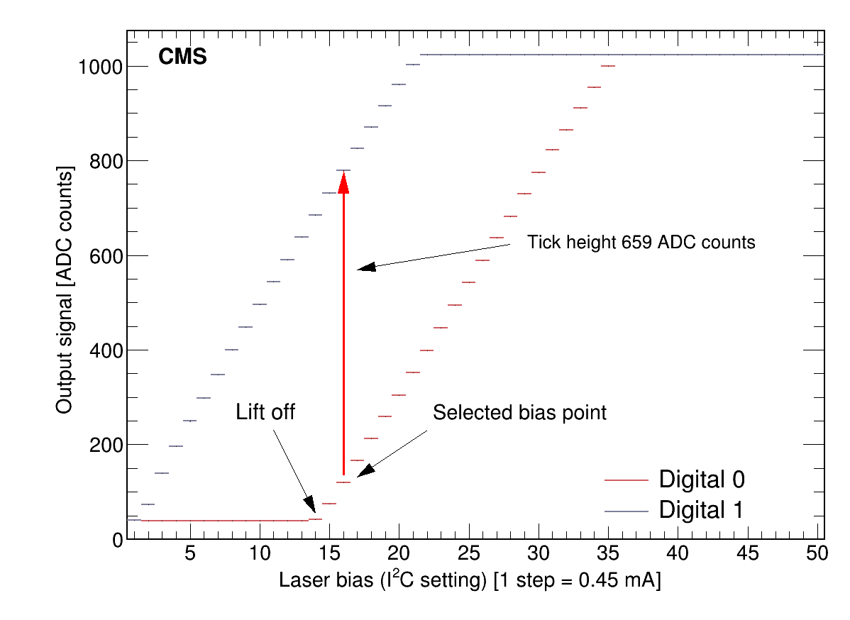
Figure 10:
Chosen gain settings at different operating temperatures. The expected migration to lower gain settings with decreasing temperature is seen. |
png pdf |
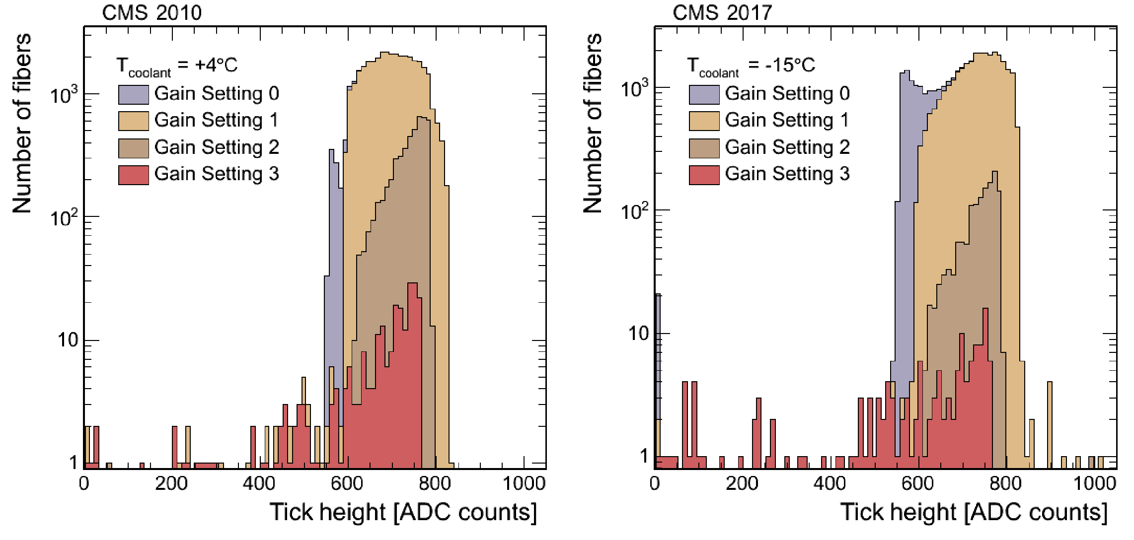
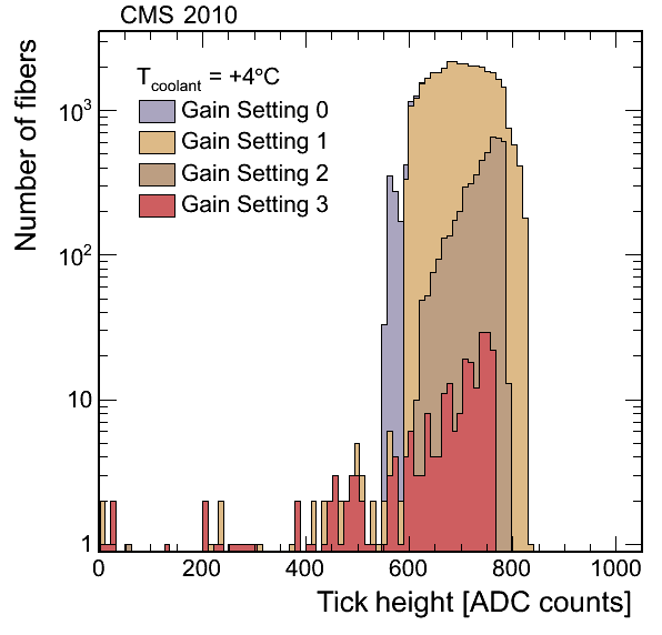
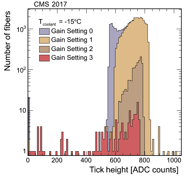
Figure 11:
Example distributions of tick heights for each of the four laser driver gain settings for data taken in 2010 at $ +4^\circ $C coolant temperature (left) and in 2017 at $ -15^\circ $C coolant temperature (right). Distributions from different gain settings are stacked. |
png |
Figure 11-a:
Example distributions of tick heights for each of the four laser driver gain settings for data taken in 2010 at $ +4^\circ $C coolant temperature (left) and in 2017 at $ -15^\circ $C coolant temperature (right). Distributions from different gain settings are stacked. |
png |
Figure 11-b:
Example distributions of tick heights for each of the four laser driver gain settings for data taken in 2010 at $ +4^\circ $C coolant temperature (left) and in 2017 at $ -15^\circ $C coolant temperature (right). Distributions from different gain settings are stacked. |
png pdf |
Figure 12:
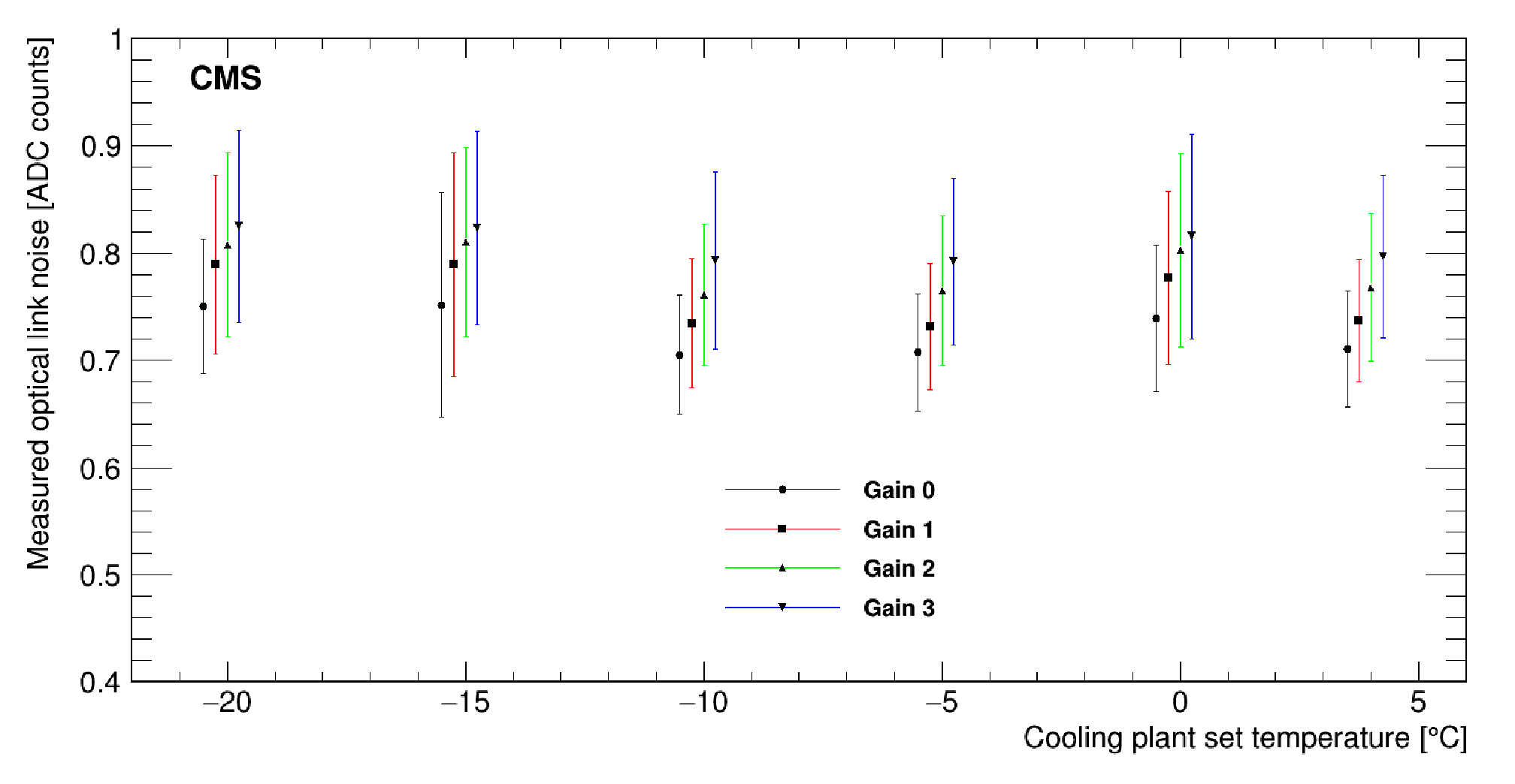
Noise measured in the optical link chain during optical link setup runs at temperatures between $ +4^\circ $C and $ -20^\circ $C coolant temperature for the four laser driver gain settings. The error bars show the root-mean-square (RMS) of the individual noise distributions and are a measure of the spread of the noise among all optical links in the SST. Points for different gain settings at the same temperature are slightly displaced for visibility. |
png pdf |
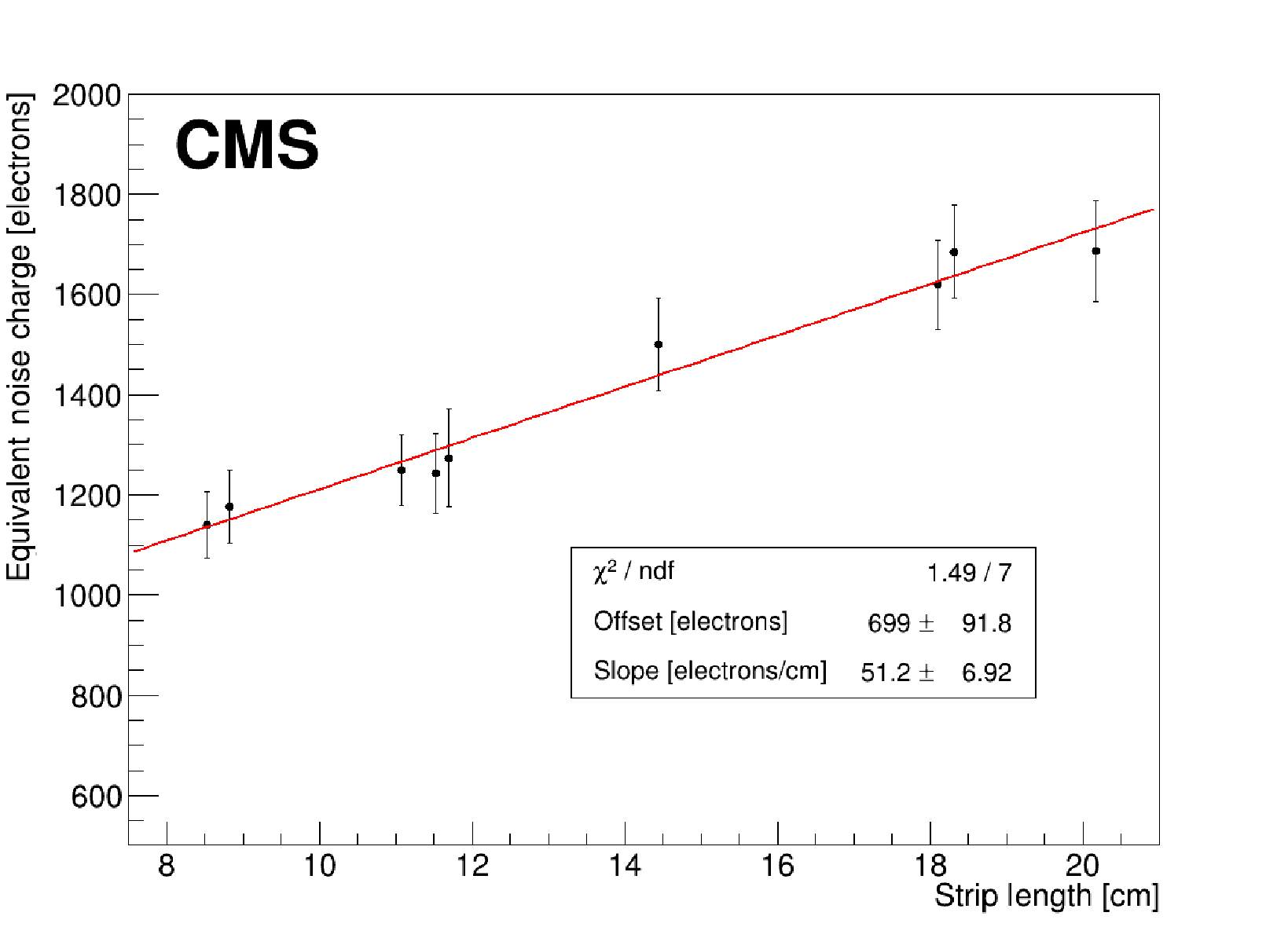
Figure 13:
Equivalent noise charge as a function of the strip length. |
png pdf |
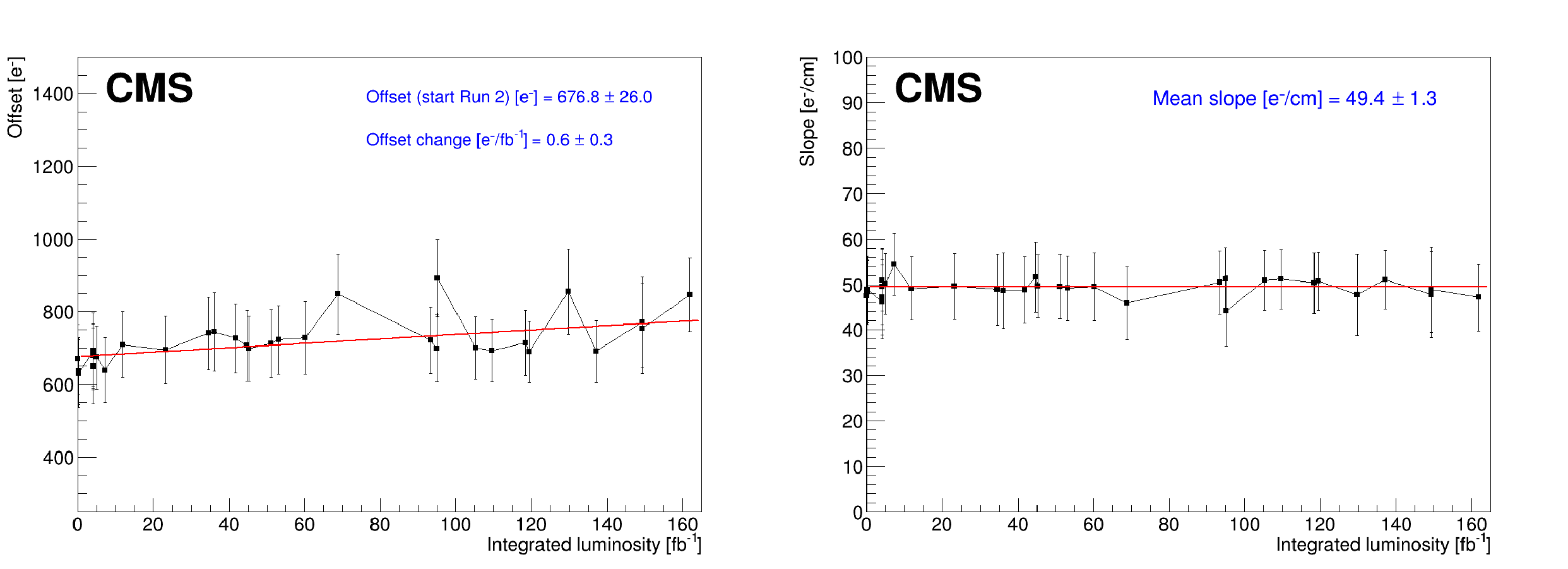
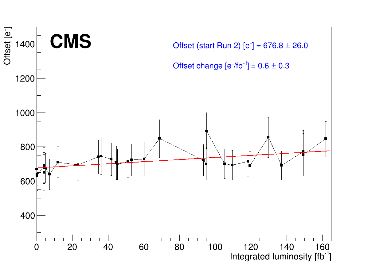
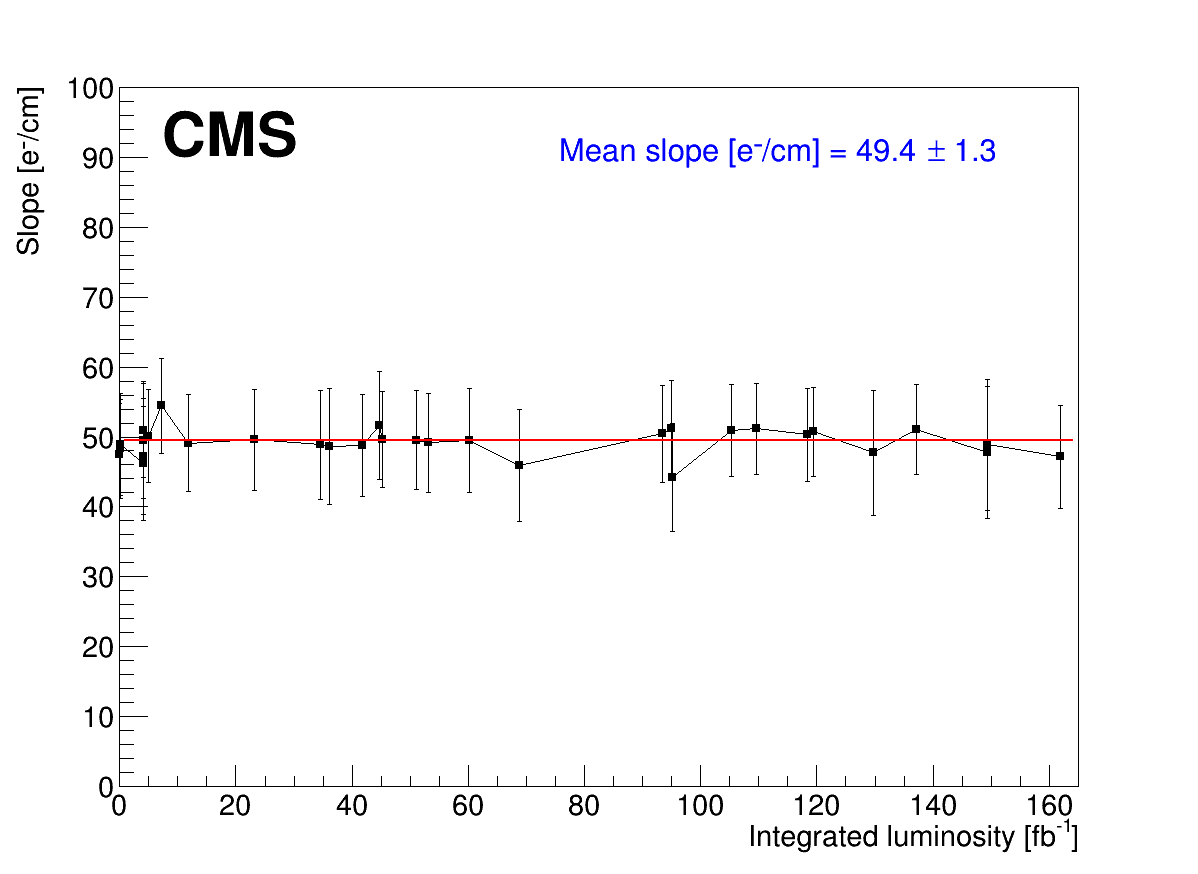
Figure 14:
Offsets (left) and slopes (right) as a function of the integrated luminosity, derived from straight-line fits to the equivalent noise charge as a function of the strip length. |
png |
Figure 14-a:
Offsets (left) and slopes (right) as a function of the integrated luminosity, derived from straight-line fits to the equivalent noise charge as a function of the strip length. |
png |
Figure 14-b:
Offsets (left) and slopes (right) as a function of the integrated luminosity, derived from straight-line fits to the equivalent noise charge as a function of the strip length. |
png pdf |
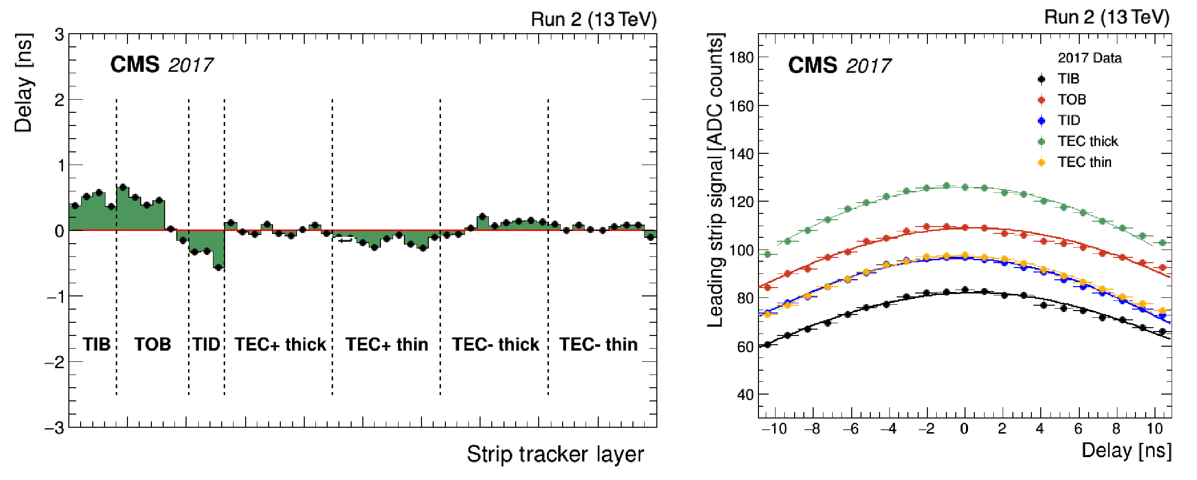
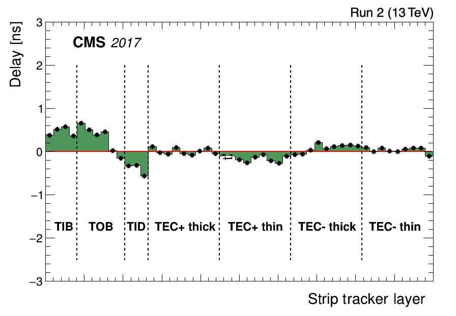
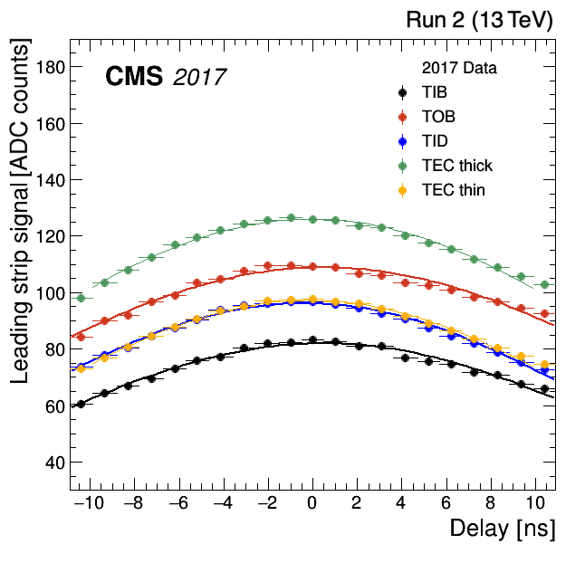
Figure 15:
Left: average delay adjustment relative to the original sampling point for each layer of the tracker. Right: leading strip charge in a cluster as function of the change in sampling point for different parts of the strip tracker. The data are fit with a Gaussian function to determine the position of the maximum. The smallest possible delay adjustment is 1\unitns. |
png |
Figure 15-a:
Left: average delay adjustment relative to the original sampling point for each layer of the tracker. Right: leading strip charge in a cluster as function of the change in sampling point for different parts of the strip tracker. The data are fit with a Gaussian function to determine the position of the maximum. The smallest possible delay adjustment is 1\unitns. |
png |
Figure 15-b:
Left: average delay adjustment relative to the original sampling point for each layer of the tracker. Right: leading strip charge in a cluster as function of the change in sampling point for different parts of the strip tracker. The data are fit with a Gaussian function to determine the position of the maximum. The smallest possible delay adjustment is 1\unitns. |
png pdf |
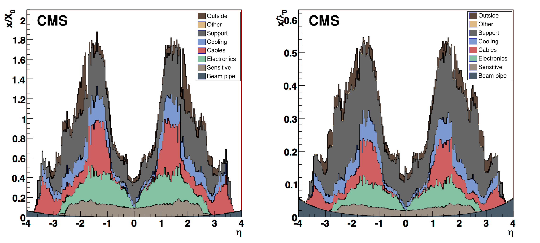
Figure 16:
Material budget in units of radiation length (left) and interaction length (right) as a function of $ \eta $ in the SST simulation, shown for the different material categories: beam pipe, silicon sensitive volumes, electronics, cables, cooling pipes and fluid, support mechanics and outside structures (support tube, thermal screen and bulkheads). |
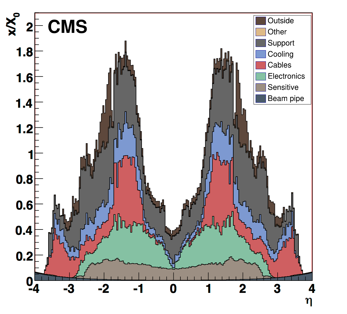
png |
Figure 16-a:
Material budget in units of radiation length (left) and interaction length (right) as a function of $ \eta $ in the SST simulation, shown for the different material categories: beam pipe, silicon sensitive volumes, electronics, cables, cooling pipes and fluid, support mechanics and outside structures (support tube, thermal screen and bulkheads). |
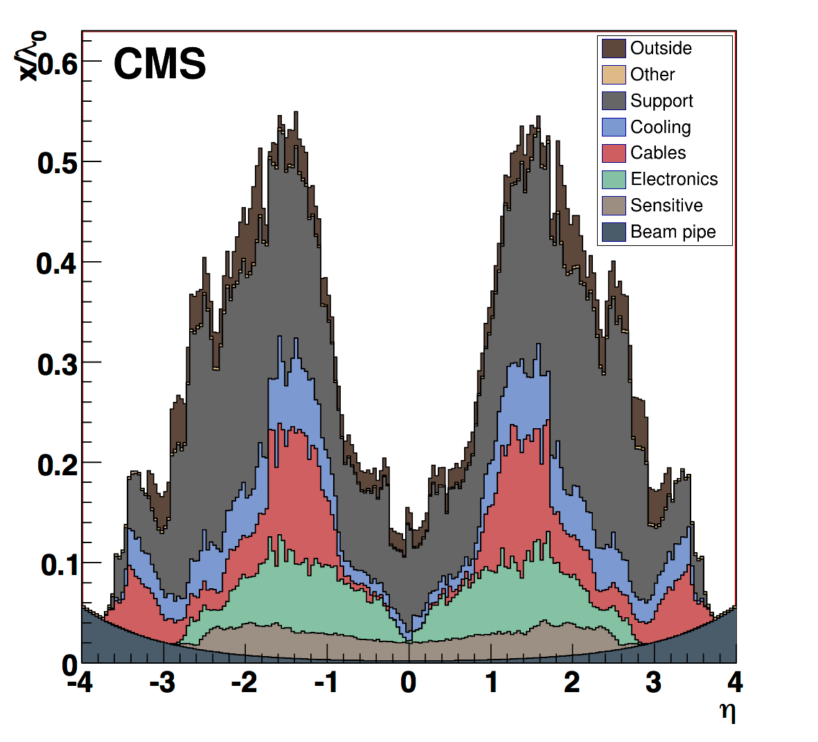
png |
Figure 16-b:
Material budget in units of radiation length (left) and interaction length (right) as a function of $ \eta $ in the SST simulation, shown for the different material categories: beam pipe, silicon sensitive volumes, electronics, cables, cooling pipes and fluid, support mechanics and outside structures (support tube, thermal screen and bulkheads). |
png pdf |
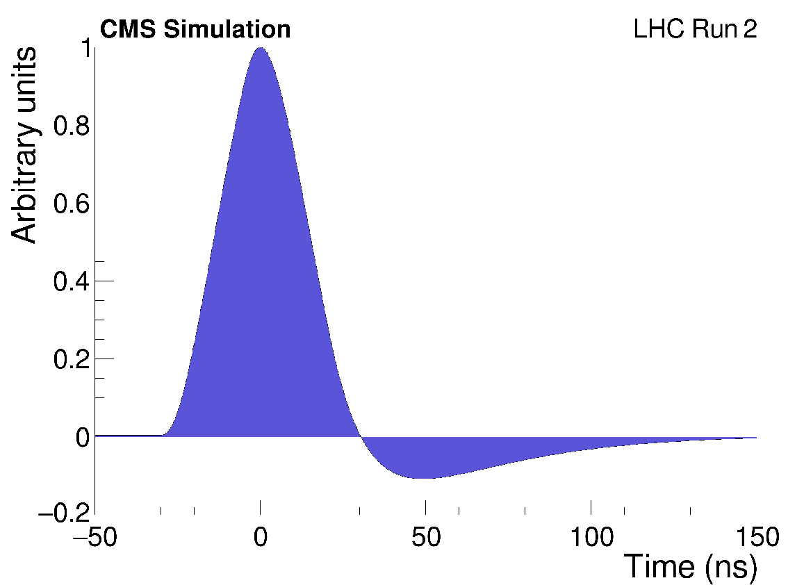
Figure 17:
Simulated APV25 pulse shape (deconvolution mode) in the CMS simulation software. The peak is centered at 0, corresponding to a perfect timing alignment with respect to LHC collisions. |
png pdf |
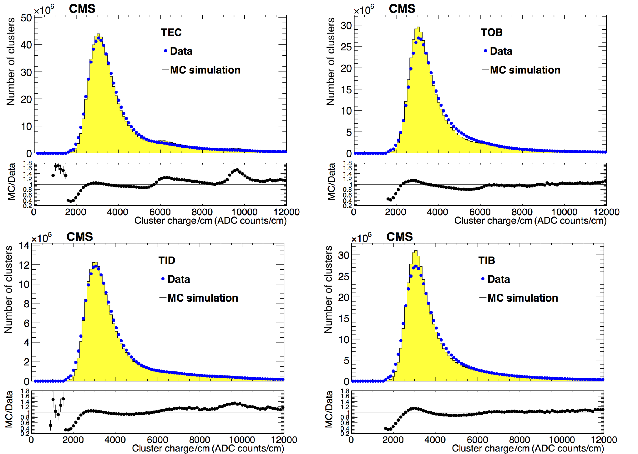
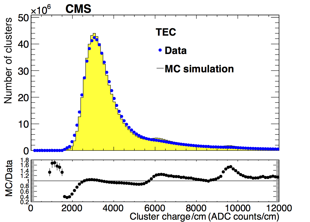
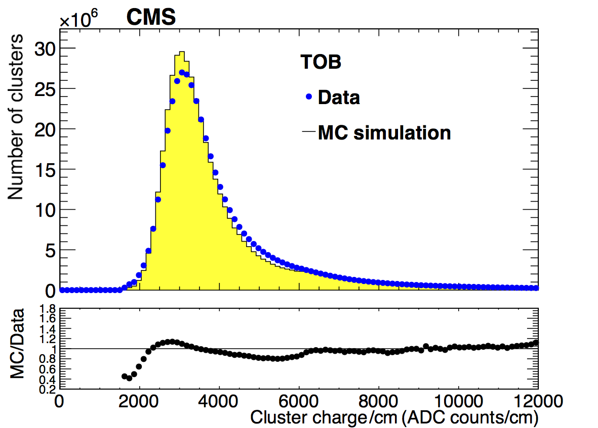
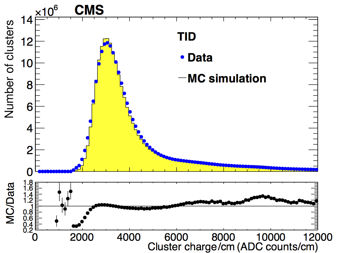
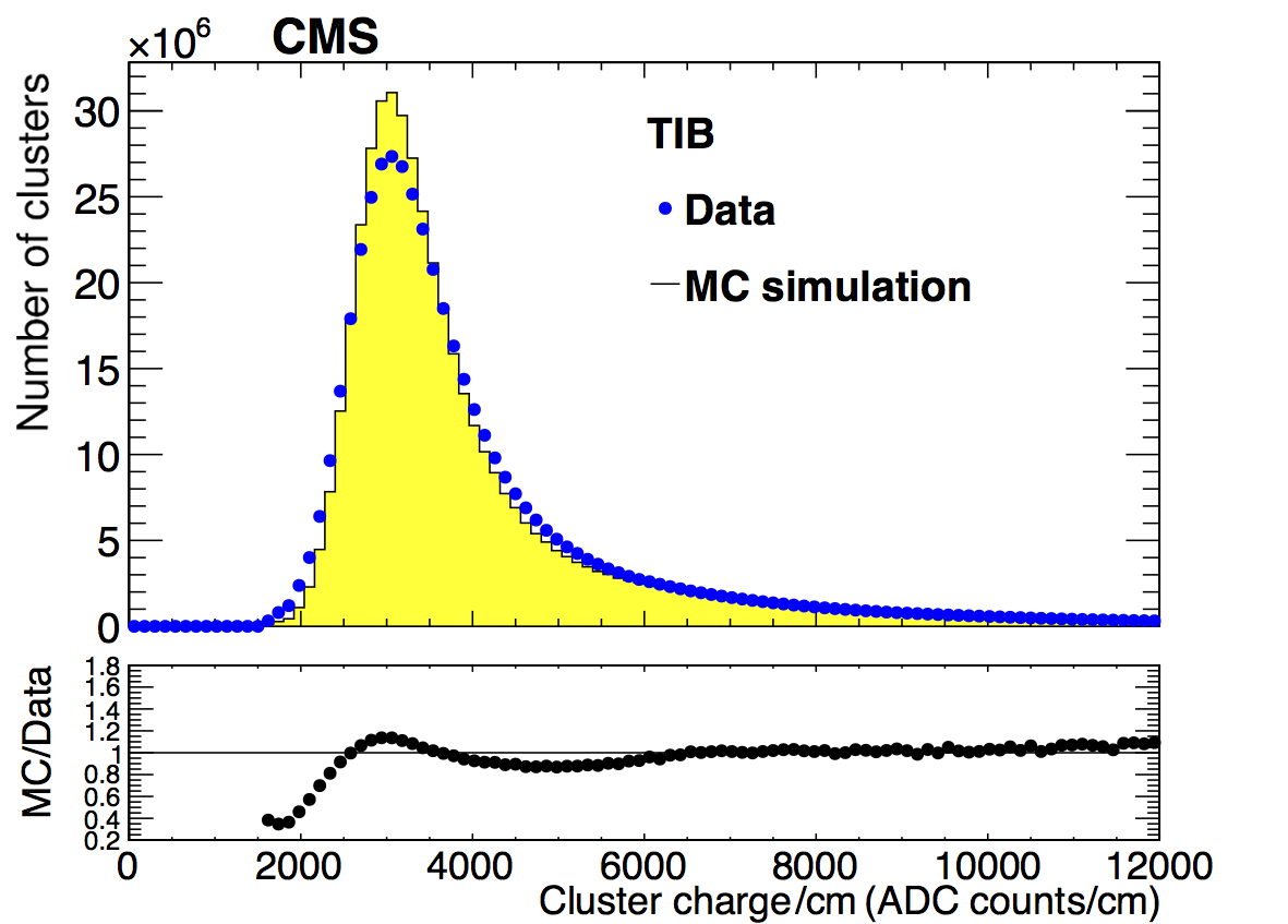
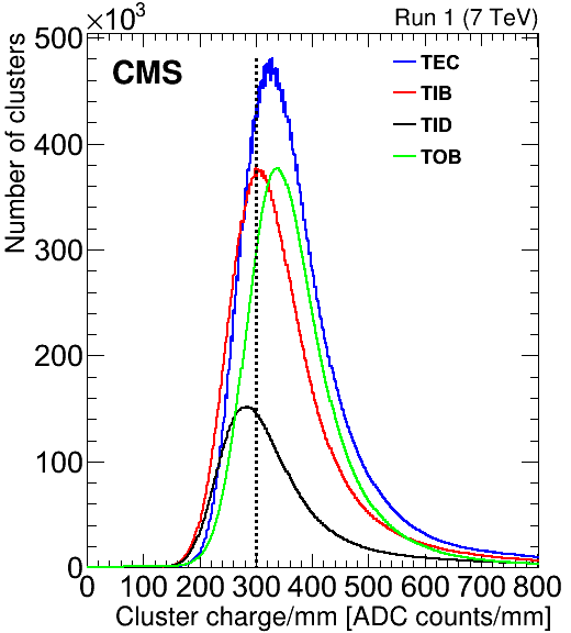
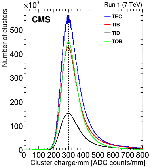
Figure 18:
Simulated and measured cluster charge normalized with the track path length for the different SST subdetectors: TEC (upper left), TOB (upper right), TID (lower left), and TIB (lower right). The measurements are shown by points, whereas the simulations are shown by yellow histograms. Lower panels show the ratios of the simulated predictions to data. |
png |
Figure 18-a:
Simulated and measured cluster charge normalized with the track path length for the different SST subdetectors: TEC (upper left), TOB (upper right), TID (lower left), and TIB (lower right). The measurements are shown by points, whereas the simulations are shown by yellow histograms. Lower panels show the ratios of the simulated predictions to data. |
png |
Figure 18-b:
Simulated and measured cluster charge normalized with the track path length for the different SST subdetectors: TEC (upper left), TOB (upper right), TID (lower left), and TIB (lower right). The measurements are shown by points, whereas the simulations are shown by yellow histograms. Lower panels show the ratios of the simulated predictions to data. |
png |
Figure 18-c:
Simulated and measured cluster charge normalized with the track path length for the different SST subdetectors: TEC (upper left), TOB (upper right), TID (lower left), and TIB (lower right). The measurements are shown by points, whereas the simulations are shown by yellow histograms. Lower panels show the ratios of the simulated predictions to data. |
png |
Figure 18-d:
Simulated and measured cluster charge normalized with the track path length for the different SST subdetectors: TEC (upper left), TOB (upper right), TID (lower left), and TIB (lower right). The measurements are shown by points, whereas the simulations are shown by yellow histograms. Lower panels show the ratios of the simulated predictions to data. |
png pdf |
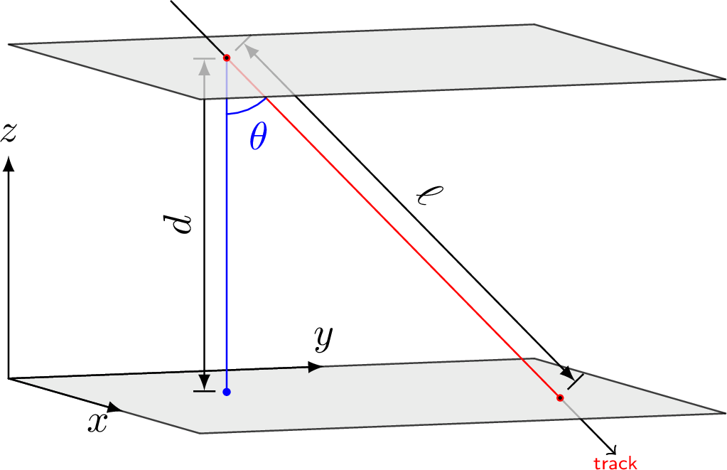
Figure 19:
Path length $ \ell $ of a particle crossing a detector of thickness $ d $ at an angle $ \theta $. |
png pdf |
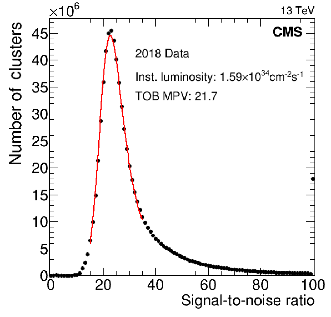
Figure 20:
Example of a signal-to-noise distribution from the TOB recorded during 2018 at an instantaneous luminosity of 1.59\ten34$ \text{cm}^{-2} \text{s}^{-1} $. The central part of the distribution is fitted with a Landau convoluted with a Gaussian distribution. The bin at 100 serves as the overflow bin. |
png pdf |
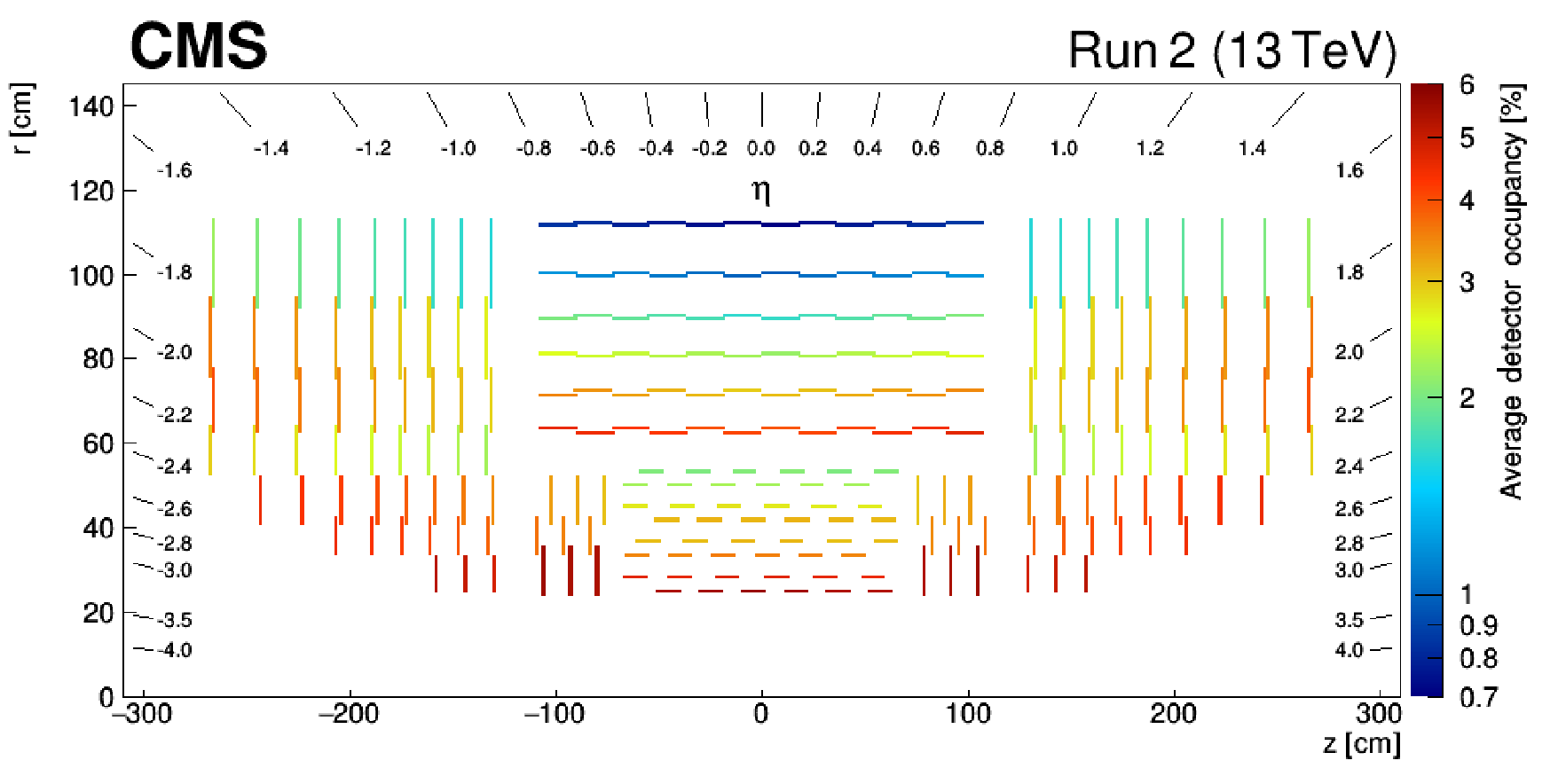
Figure 21:
View of the SST mean strip occupancy in the $ r-z $ plane recorded at the beginning of a typical LHC fill where the pileup was at its maximum (of the order of 55). |
png pdf |
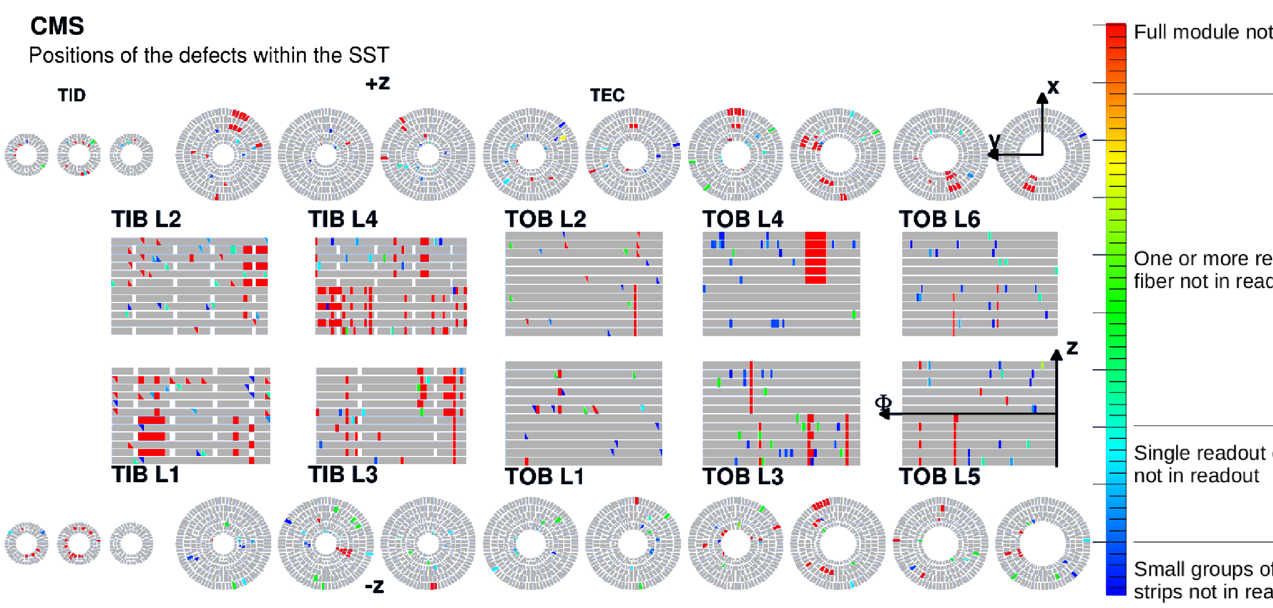
Figure 22:
Positions of the defects within the SST at the module level at the end of 2017. Disabled modules are shown in red. Those with at least one fiber not in the readout appear in green. The range blue to green indicates damage varying from single strips (dark blue) to all strips of a single chip. The total number of defects represents less than 5% of the total number of the SST channels. |
png pdf |
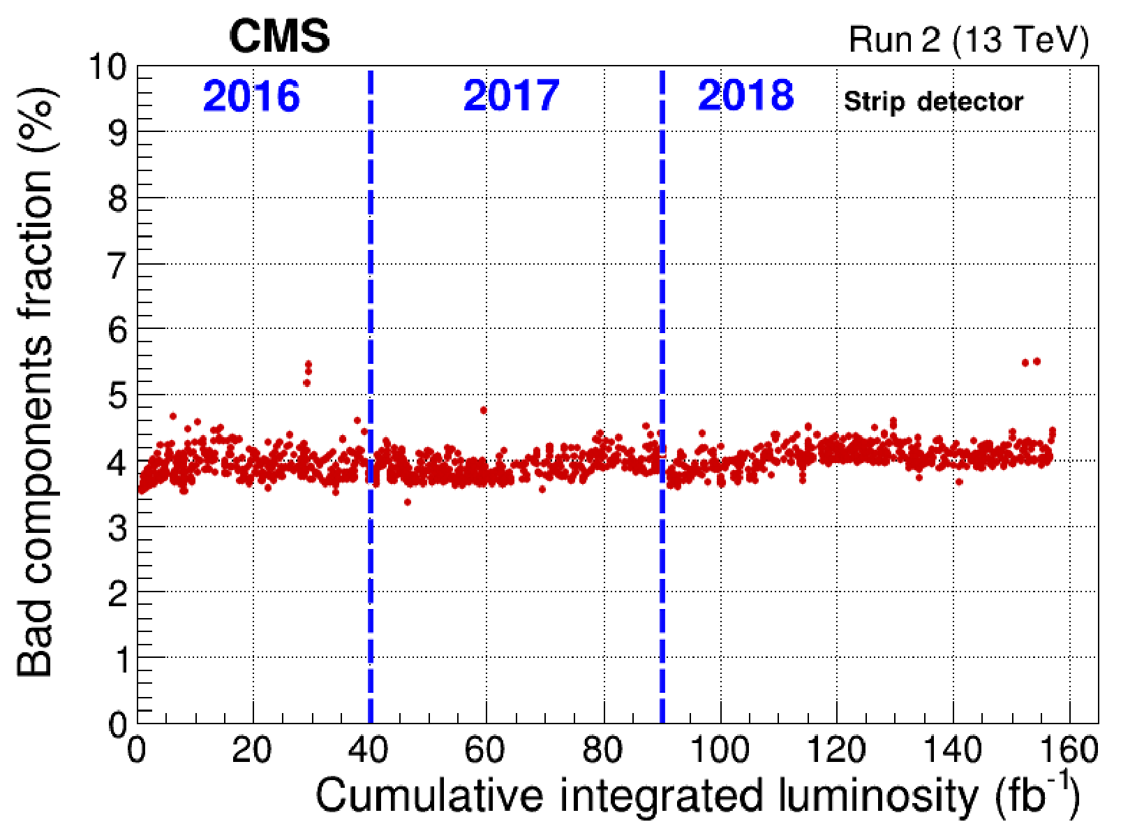
Figure 23:
Fraction of bad channels as a function of the delivered LHC integrated luminosity. The vertical lines indicate the start of each calendar year. |
png pdf |
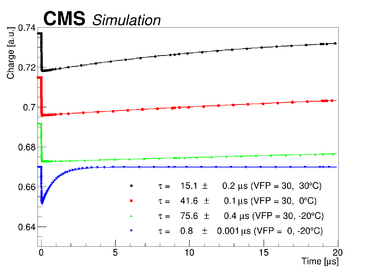
Figure 24:
Simulated discharge behavior of the APV25 preamplifier for different temperatures with preamplifier feedback voltage bias (VFP) at 30 (Run 1 and 2015--2016) and at 0 (second half of 2016--2018). An exponential decay function with a discharge time constant $ \tau $ is fitted to each set of simulated data. The resulting values for $ \tau $ are displayed in the legend. |
png pdf |
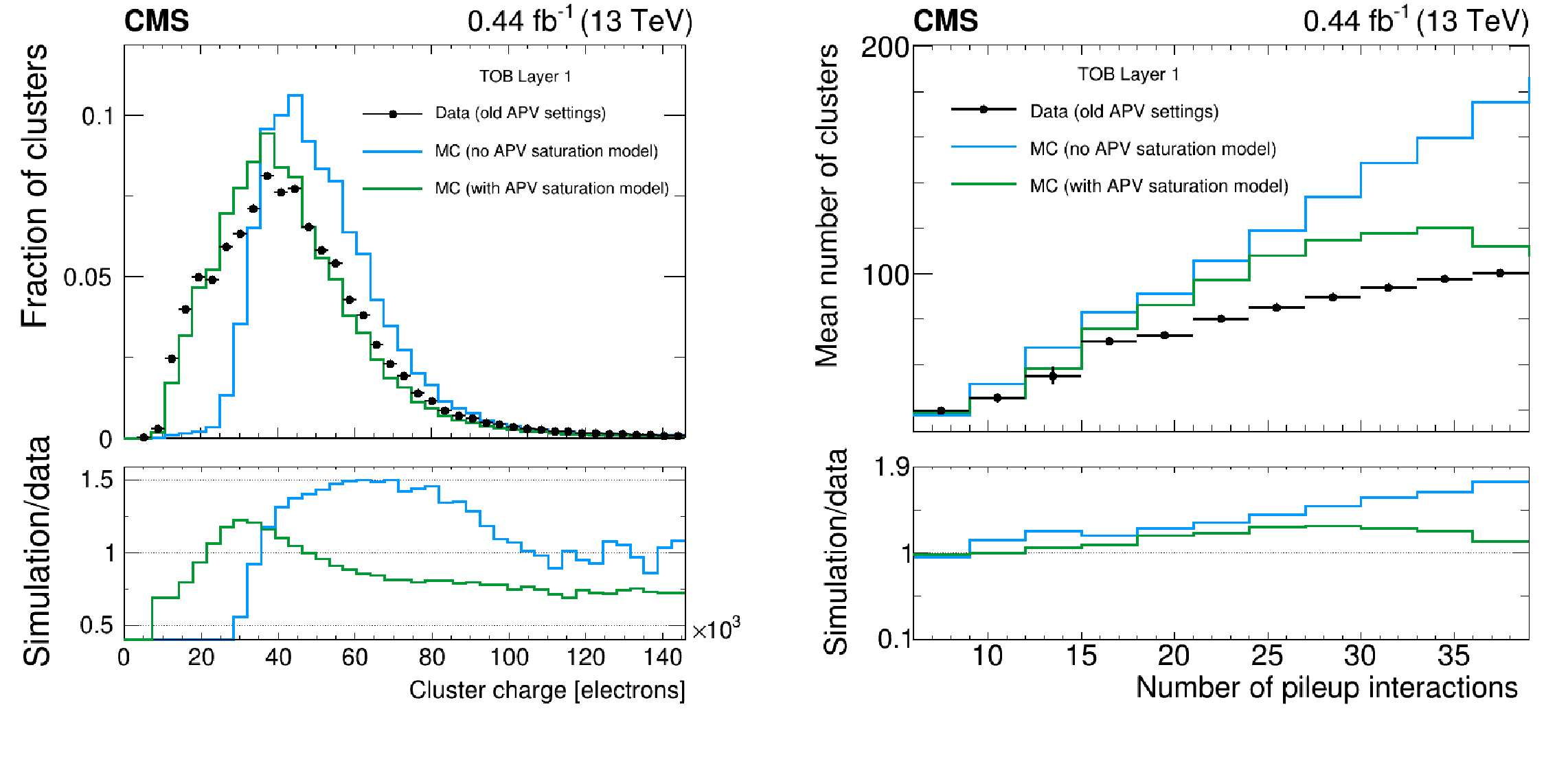
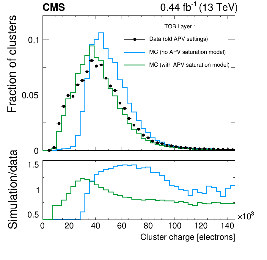
Figure 25:
Left: cluster charge distribution for clusters on reconstructed particle tracks in the TOB layer 1. Right: multiplicity of clusters on reconstructed particle tracks in the TOB layer 1 as a function of the number of pileup interactions. The data from early 2016 (black dots) are compared with two different MC simulations; one (blue) does not contain any special treatment of the APV25 preamplifier saturation, the other (green) contains a modeling of the preamplifier saturation to account for the reduced charge response of the amplifier under high-occupancy conditions. Lower panels show the ratio of MC predictions to data. |
png |
Figure 25-a:
Left: cluster charge distribution for clusters on reconstructed particle tracks in the TOB layer 1. Right: multiplicity of clusters on reconstructed particle tracks in the TOB layer 1 as a function of the number of pileup interactions. The data from early 2016 (black dots) are compared with two different MC simulations; one (blue) does not contain any special treatment of the APV25 preamplifier saturation, the other (green) contains a modeling of the preamplifier saturation to account for the reduced charge response of the amplifier under high-occupancy conditions. Lower panels show the ratio of MC predictions to data. |

png |
Figure 25-b:
Left: cluster charge distribution for clusters on reconstructed particle tracks in the TOB layer 1. Right: multiplicity of clusters on reconstructed particle tracks in the TOB layer 1 as a function of the number of pileup interactions. The data from early 2016 (black dots) are compared with two different MC simulations; one (blue) does not contain any special treatment of the APV25 preamplifier saturation, the other (green) contains a modeling of the preamplifier saturation to account for the reduced charge response of the amplifier under high-occupancy conditions. Lower panels show the ratio of MC predictions to data. |
png pdf |
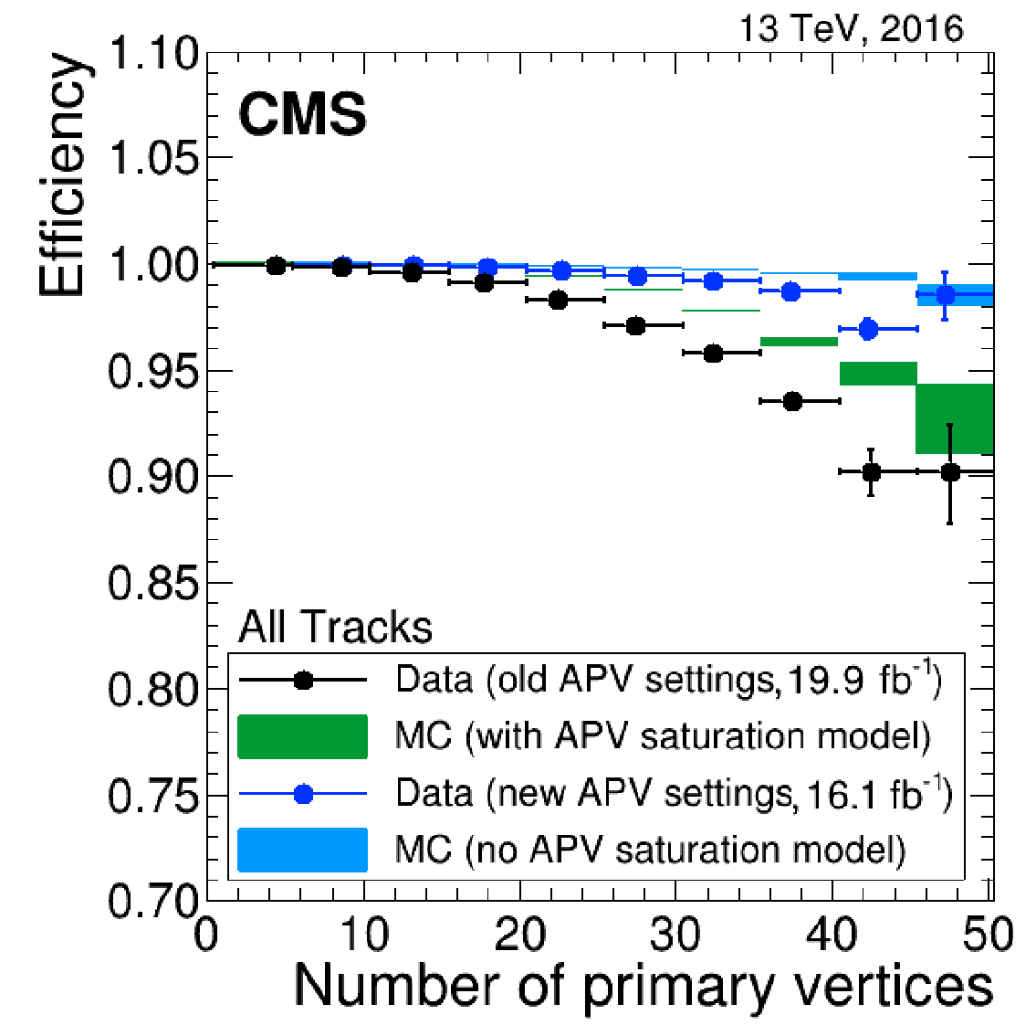
Figure 26:
Tracking efficiency estimated using a tag-and-probe method as a function of the number of primary vertices for an inclusive muon track collection [36]. Data from early 2016 (black dots) and late 2016 (blue dots) are compared with two different MC simulations: one (blue) does not contain any special treatment of the APV25 preamplifier saturation, the second (green) contains a modeling of the preamplifier saturation to account for the reduced charge response of the amplifier under high-occupancy conditions. |
png pdf |
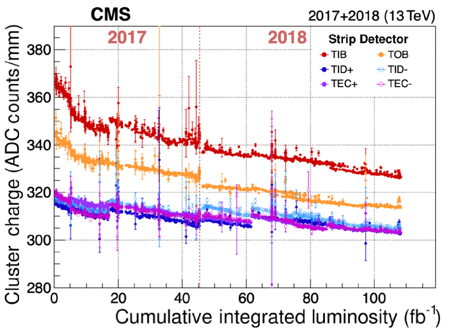
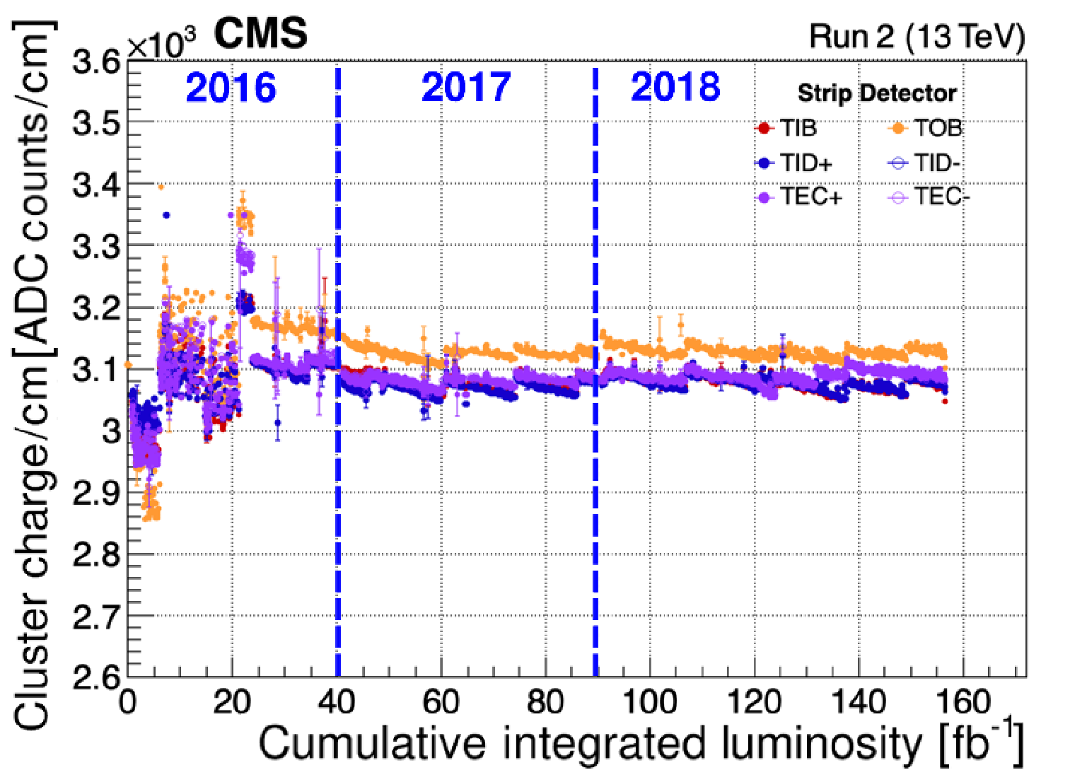
Figure 27:
Evolution of the cluster charge normalized to unit length as a function of the integrated luminosity for different parts of the SST. The zero point of the plot is after the integrated luminosities of Run 1 and the years 2015 and 2016 for a total of 75.3 fb$ ^{-1} $. |

png pdf |
Figure 28:
Signal-to-noise ratio for clusters on reconstructed particle tracks in TOB layer 1 for two runs in 2016. The first run (red curve) is affected by saturation effects in the APV25 preamplifier. In the second run (blue curve), the preamplifier voltage feedback (VFP) has been changed to shorten the discharge time of the preamplifier. Both curves are normalized to the same number of entries. |
png pdf |
Figure 29:
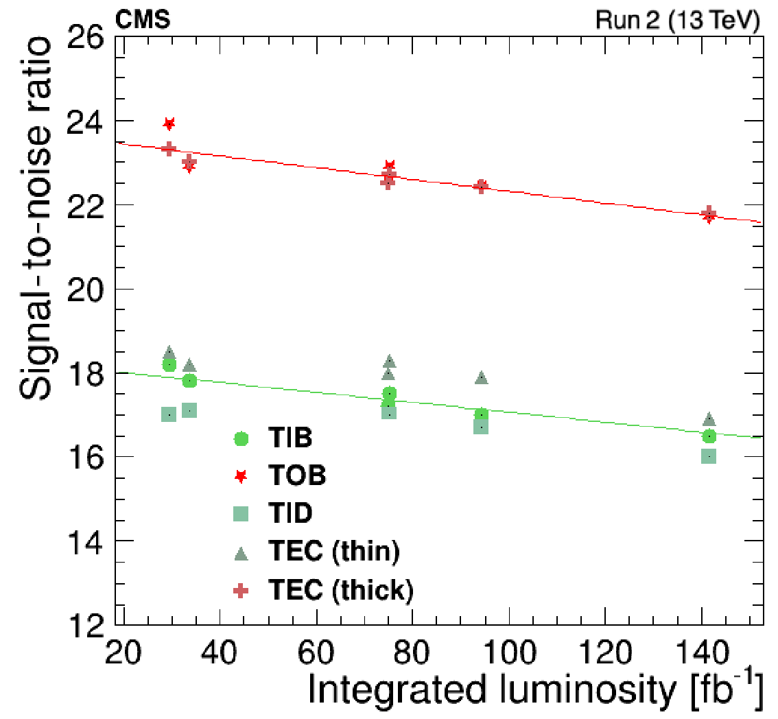
Signal-to-noise ratio as a function of the integrated luminosity for modules from different parts of the tracker. Trend lines are obtained by separately fitting a linear function to the points for thin and thick sensors. |
png pdf |
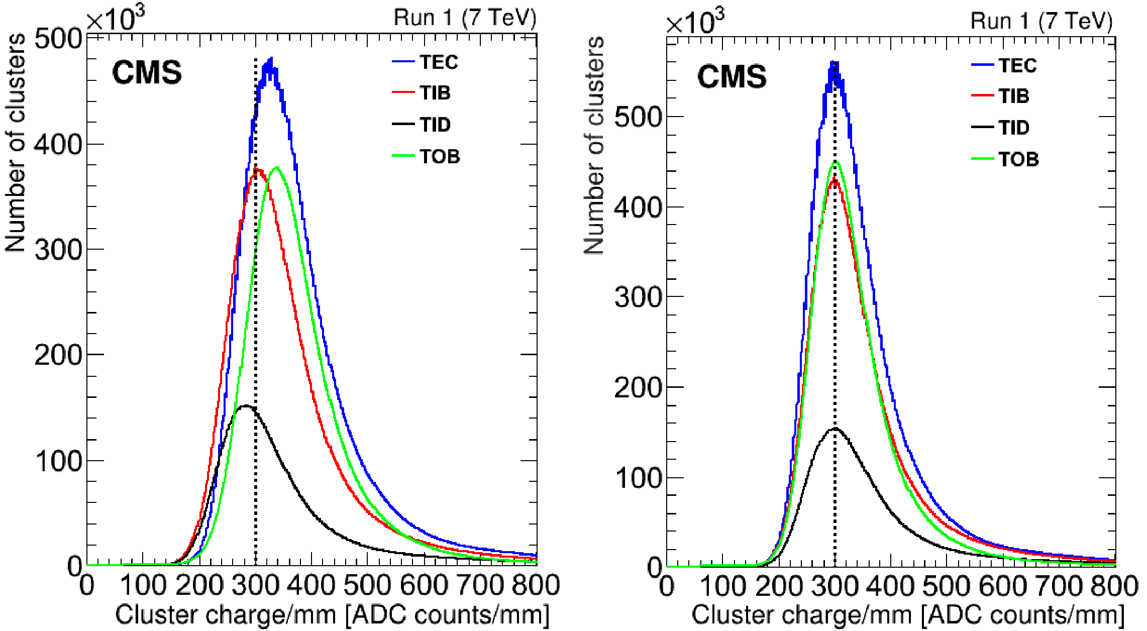
Figure 30:
The distribution of the charge normalized to the path length after the tick mark calibration before (left) and after (right) applying the signal equalization. The dashed line represents the calibration value (set to 300 ADC counts/mm). |
png |
Figure 30-a:
The distribution of the charge normalized to the path length after the tick mark calibration before (left) and after (right) applying the signal equalization. The dashed line represents the calibration value (set to 300 ADC counts/mm). |
png |
Figure 30-b:
The distribution of the charge normalized to the path length after the tick mark calibration before (left) and after (right) applying the signal equalization. The dashed line represents the calibration value (set to 300 ADC counts/mm). |
png pdf |
Figure 31:
Cluster charge normalized to the path length after the offline calibration for the SST barrel (TIB and TOB) and the plus and minus sides of the TID and TEC as a function of the delivered integrated luminosity. The vertical lines indicate the start of each calendar year. The large fluctuations in 2016 are a consequence of the APV25 saturation issue, see text for details. |
png pdf |
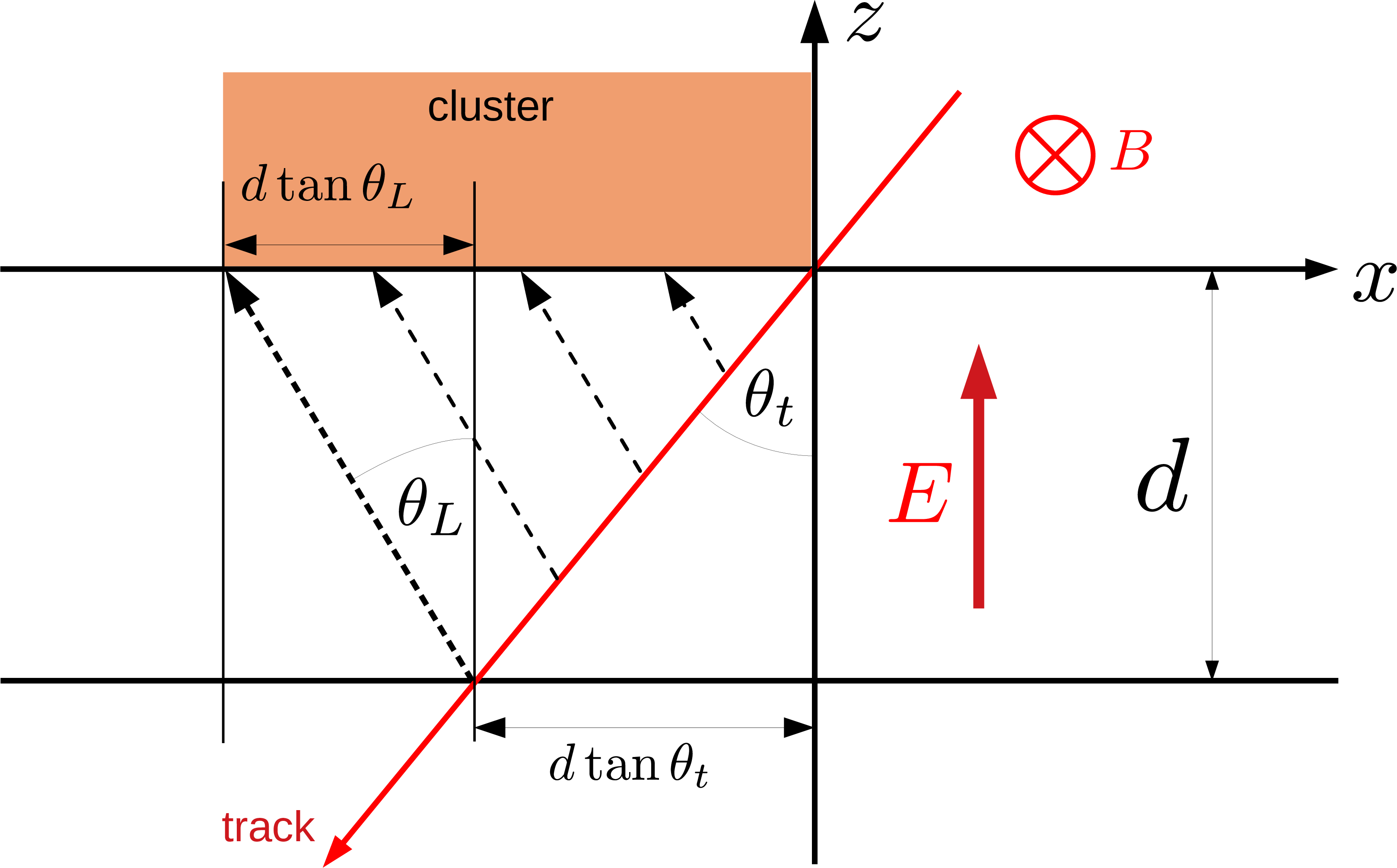
Figure 32:
Illustration of the shift due to the Lorentz force along the sensitive coordinate $ x $ of a sensor of thickness $ d $. The Lorentz angle is $ \theta_{\mathrm{L}} $ and the $ z $ axis is perpendicular to the sensor. The particle crosses the sensor with an incident angle $ \theta_{\mathrm{t}} $. The dashed arrows represent the direction of drift of charge carriers produced in the silicon. The cluster is represented by the orange rectangle. The cluster size $ d \tan\theta_{\mathrm{t}} $ is increased by $ d \tan\theta_{\mathrm{L}} $ in the presence of the magnetic field. |
png pdf |
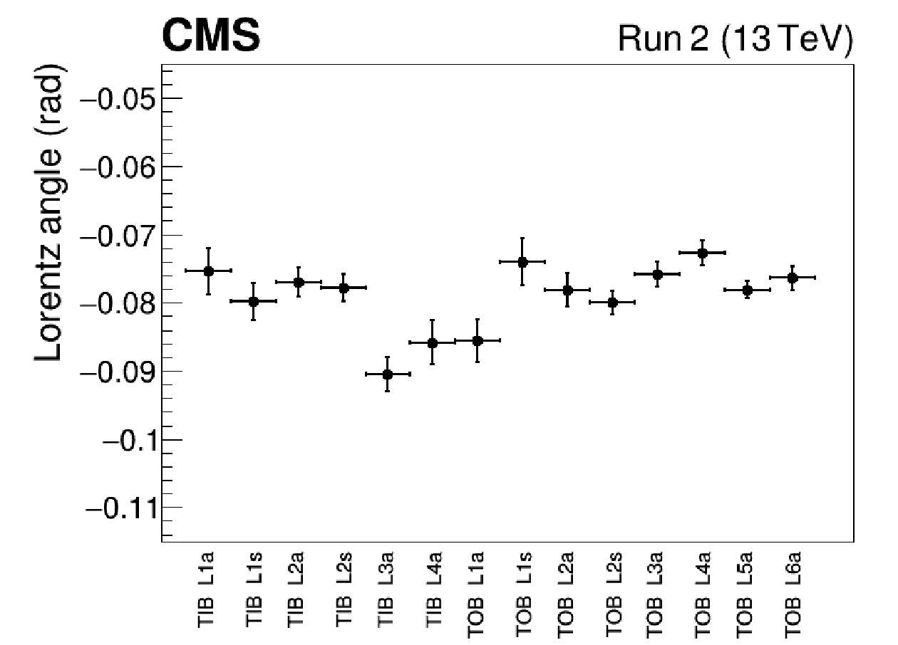
Figure 33:
Lorentz angle measured at the end of Run 2 for the different SST layers of the TIB and TOB. The measurement is displayed separately for modules with strips oriented along the $ z $ direction, labeled a, and modules with the strips rotated by an angle of 100 mrad with respect to the $ z $ direction, labeled s. |
png pdf |
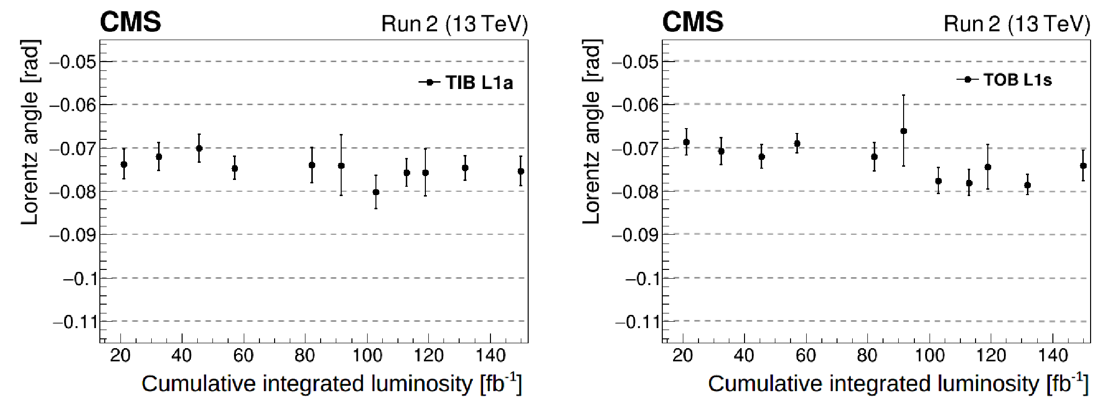
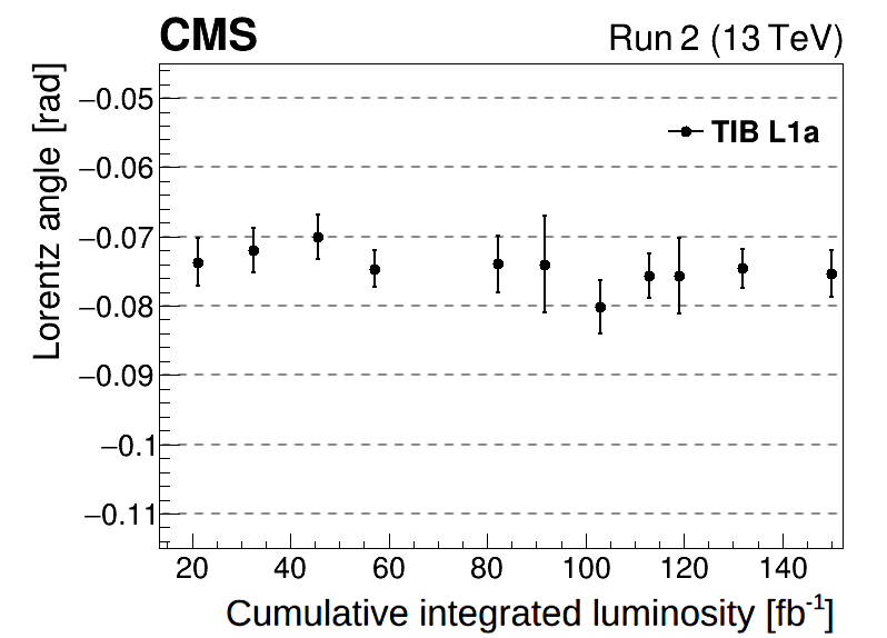
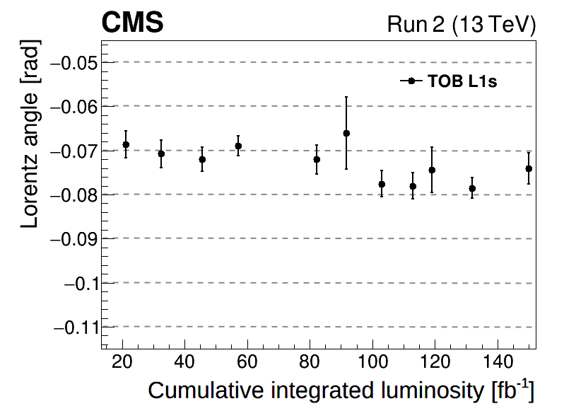
Figure 34:
Evolution of the Lorentz angle during Run 2, for modules with strips oriented along the $ z $ direction belonging to the first layer of the TIB, L1a (left), and for modules with the strips rotated by an angle of 100 mrad with respect to the $ z $ direction belonging to the TOB, L1s (right). The dashed lines are drawn to guide the eye. |
png |
Figure 34-a:
Evolution of the Lorentz angle during Run 2, for modules with strips oriented along the $ z $ direction belonging to the first layer of the TIB, L1a (left), and for modules with the strips rotated by an angle of 100 mrad with respect to the $ z $ direction belonging to the TOB, L1s (right). The dashed lines are drawn to guide the eye. |
png |
Figure 34-b:
Evolution of the Lorentz angle during Run 2, for modules with strips oriented along the $ z $ direction belonging to the first layer of the TIB, L1a (left), and for modules with the strips rotated by an angle of 100 mrad with respect to the $ z $ direction belonging to the TOB, L1s (right). The dashed lines are drawn to guide the eye. |
png pdf |
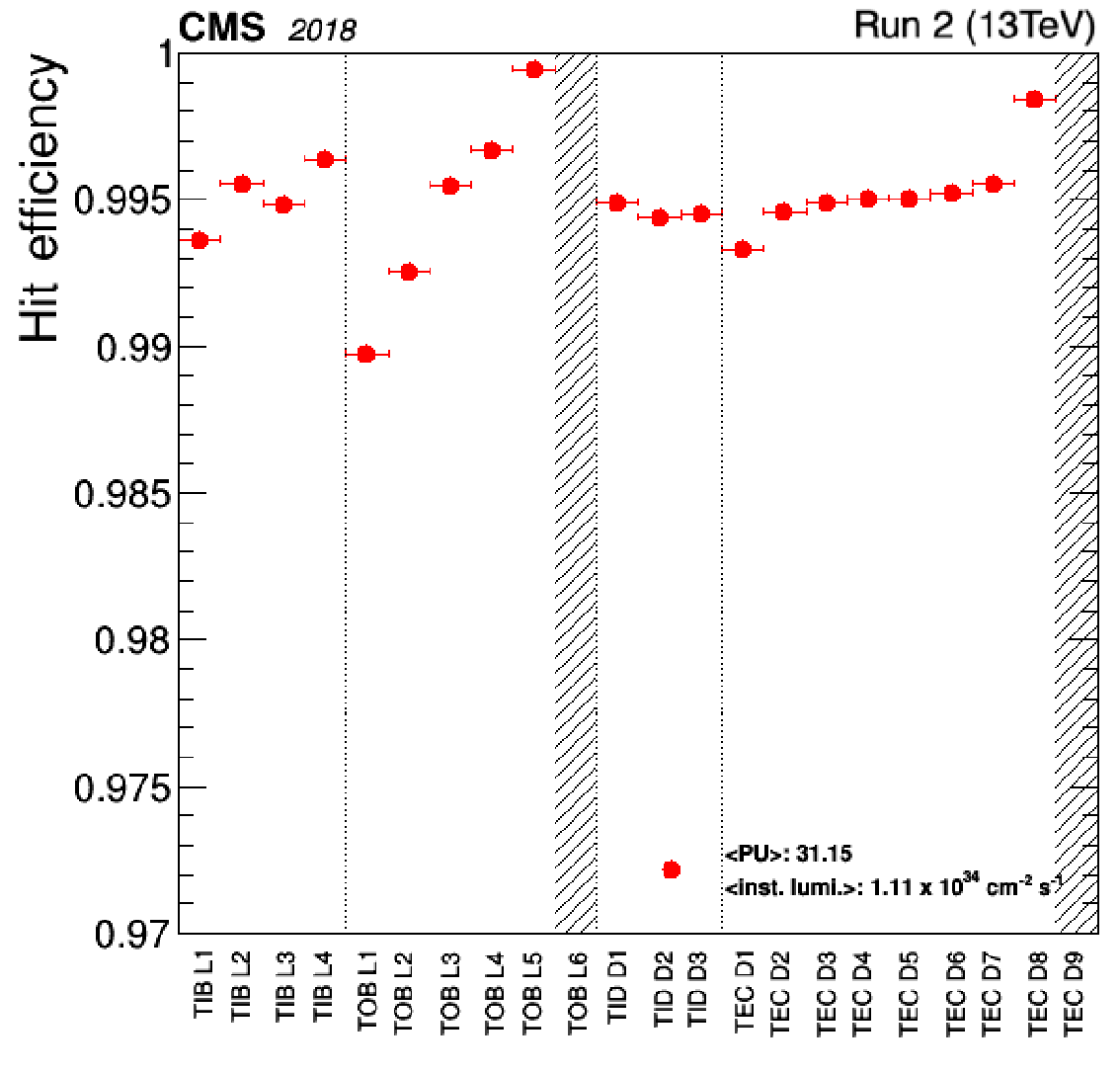
Figure 35:
Hit efficiency for the various layers of the SST at the end of Run 2. Known faulty modules are masked. The two gray bands correspond to the outermost layers where the efficiency cannot be measured. |
png pdf |
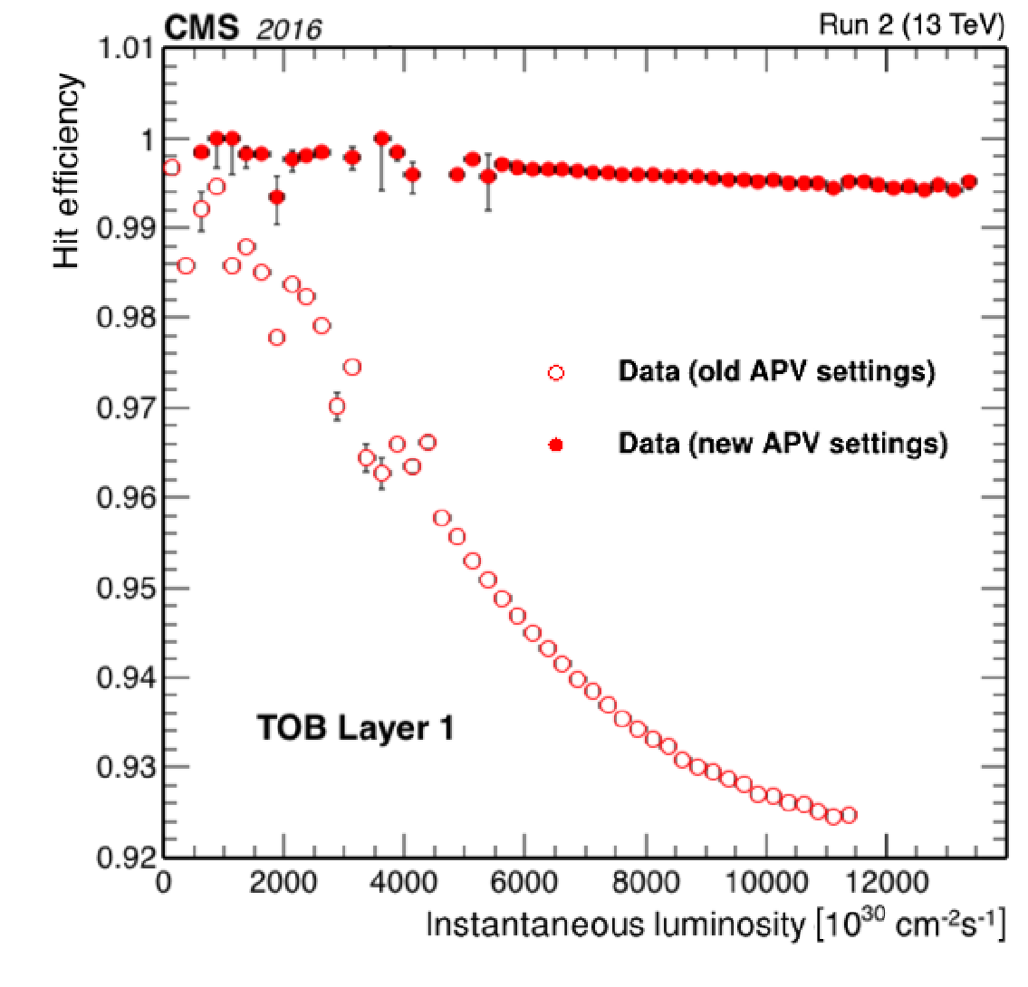
Figure 36:
Hit efficiency as a function of the instantaneous luminosity for the modules in the TOB layer 1 for runs before (open circles) and after (filled circles) the change of the APV25 preamplifier discharge speed. Error bars are statistical only. |
png pdf |
Figure 37:
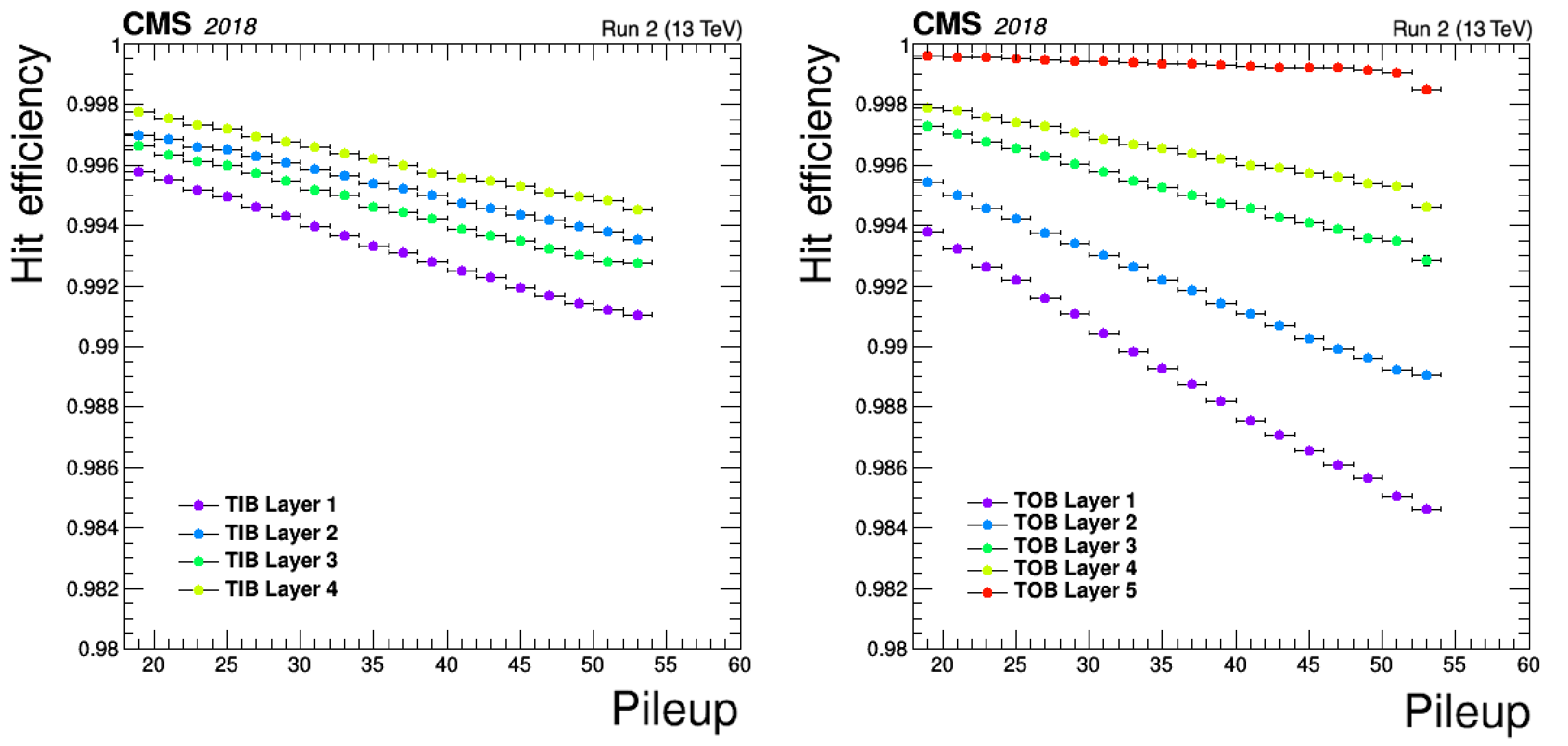
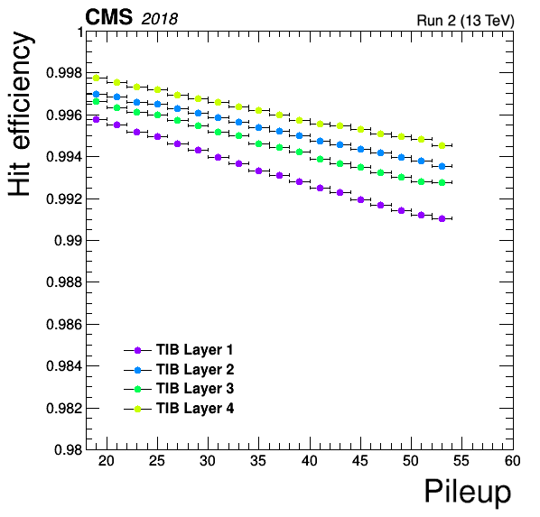
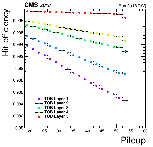
Hit efficiency for different layers in the TIB (left) and TOB (right) as a function of the average pileup multiplicity. |
png |
Figure 37-a:
Hit efficiency for different layers in the TIB (left) and TOB (right) as a function of the average pileup multiplicity. |
png |
Figure 37-b:
Hit efficiency for different layers in the TIB (left) and TOB (right) as a function of the average pileup multiplicity. |
png pdf |
Figure 38:
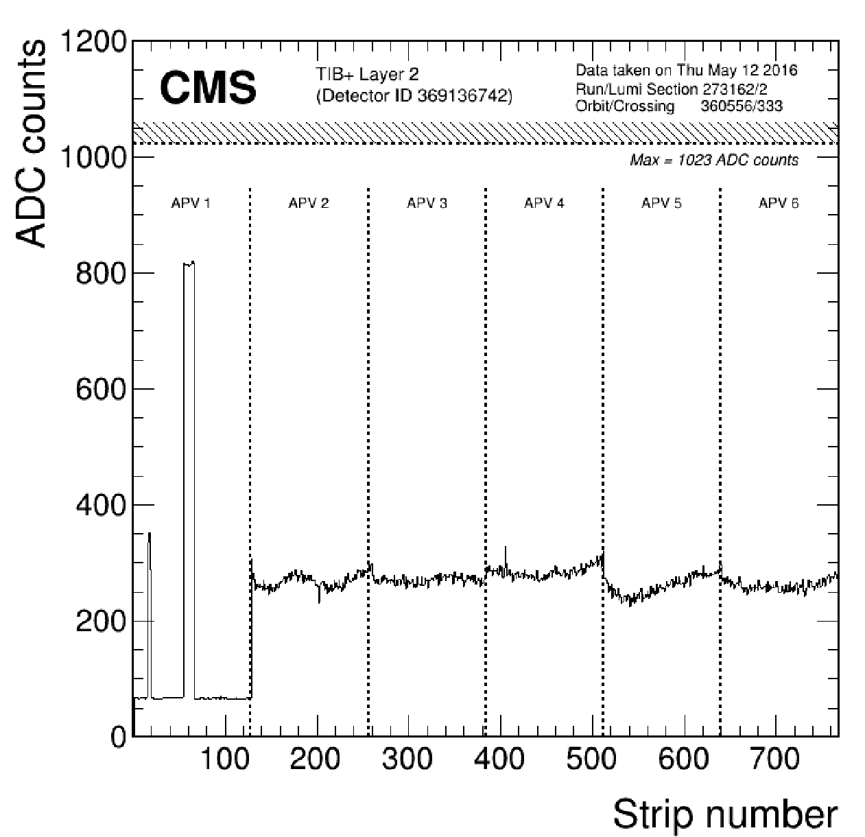
ADC counts of the six APV25 chips in a TIB module during a collision in 2016. The large charge (at $ \approx $ 800 ADC counts located around strip number $ \approx $ 60) together with a drop of the baseline in the first chip is the signature of a HIP event. |
png pdf |
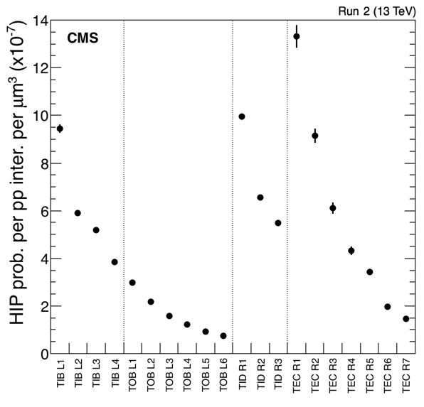
Figure 39:
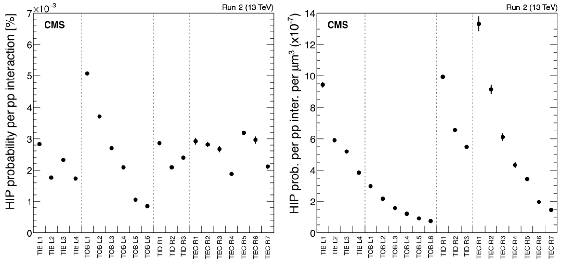
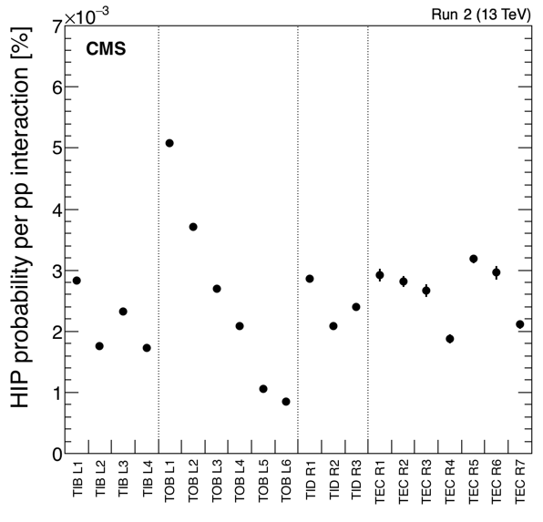
Average probability of HIP event occurrence per pp interaction (left) and normalized to unit volume (right) for all layers of the silicon strip tracker. In the endcaps, the probability is reported per ring. |
png |
Figure 39-a:
Average probability of HIP event occurrence per pp interaction (left) and normalized to unit volume (right) for all layers of the silicon strip tracker. In the endcaps, the probability is reported per ring. |
png |
Figure 39-b:
Average probability of HIP event occurrence per pp interaction (left) and normalized to unit volume (right) for all layers of the silicon strip tracker. In the endcaps, the probability is reported per ring. |
png pdf |
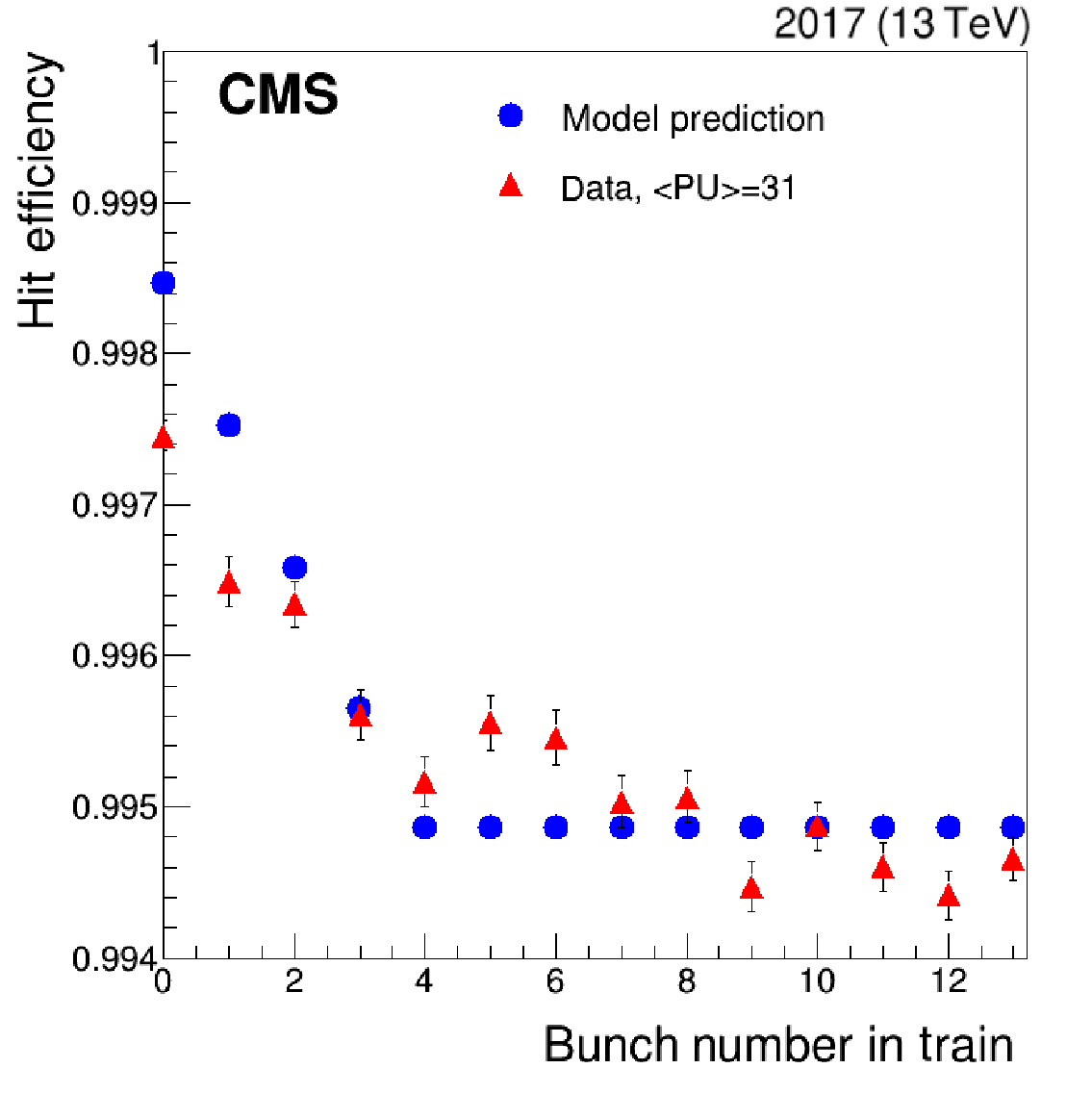
Figure 40:
Evolution of the hit efficiency as a function of bunch number within the train for TIB layer 1 modules, obtained from a representative selection of CMS 2017 data with an average pileup of 31. Bunches are separated by 25\unitns. The data are represented by red triangles and the model prediction is shown with blue circles. |
png pdf |
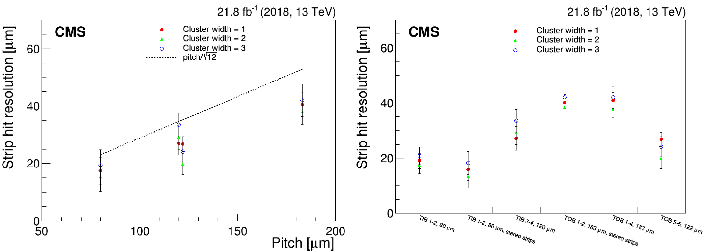
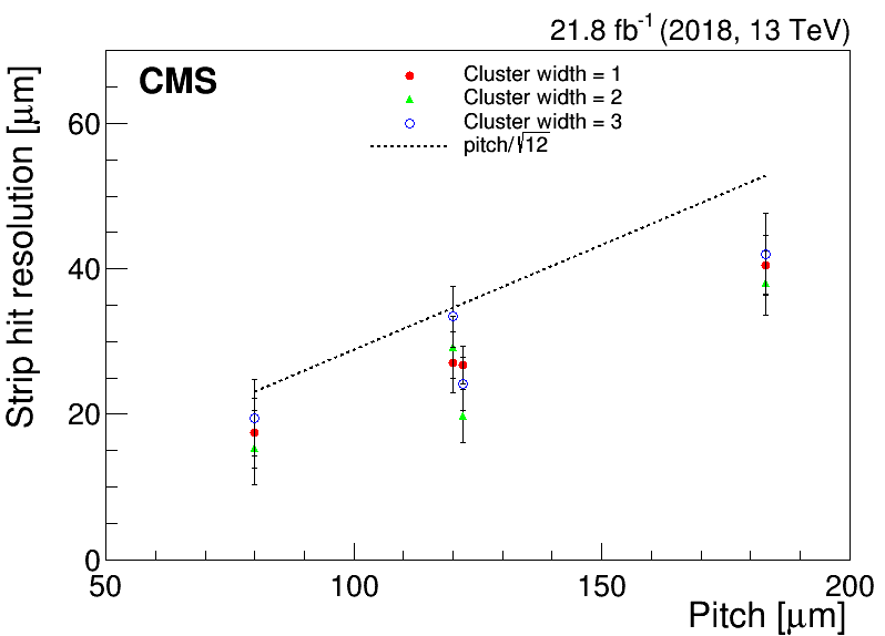
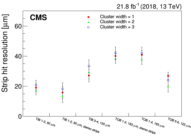
Figure 41:
Single-hit resolution as a function of the strip pitch (left) and for different detector regions (right). In the left plot, the expected resolution for binary readout (pitch/$ \sqrt{12} $) is also shown for comparison. |
png |
Figure 41-a:
Single-hit resolution as a function of the strip pitch (left) and for different detector regions (right). In the left plot, the expected resolution for binary readout (pitch/$ \sqrt{12} $) is also shown for comparison. |
png |
Figure 41-b:
Single-hit resolution as a function of the strip pitch (left) and for different detector regions (right). In the left plot, the expected resolution for binary readout (pitch/$ \sqrt{12} $) is also shown for comparison. |
png pdf |
Figure 42:
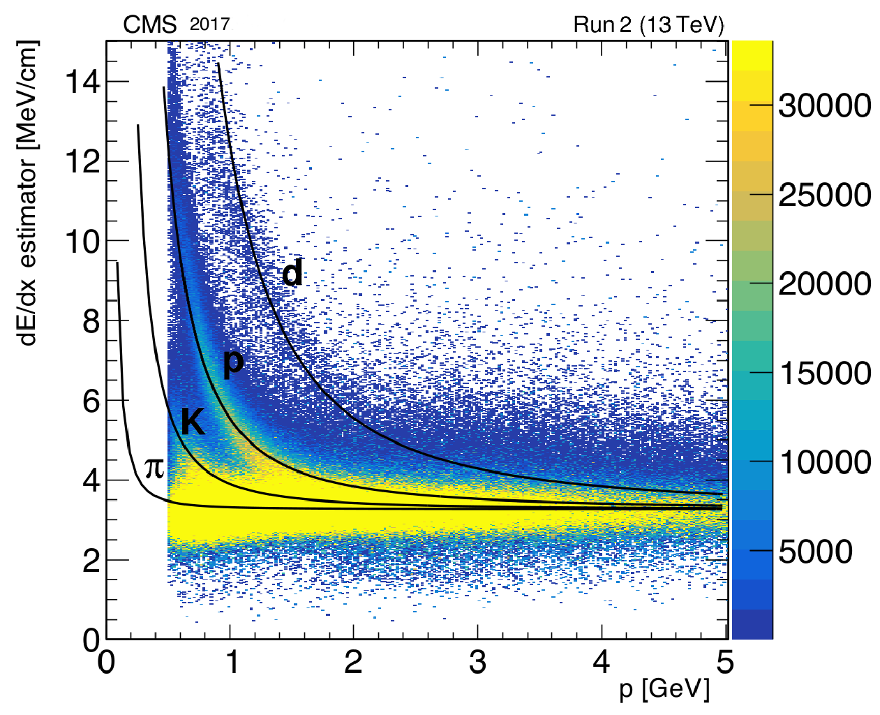
Energy loss measurement in the SST during LHC Run 2. Expected losses for pion, kaon, proton, and deuteron particles are also shown (black lines). Tracks with momentum below 0.5 GeV are not included in this plot. |
png pdf |
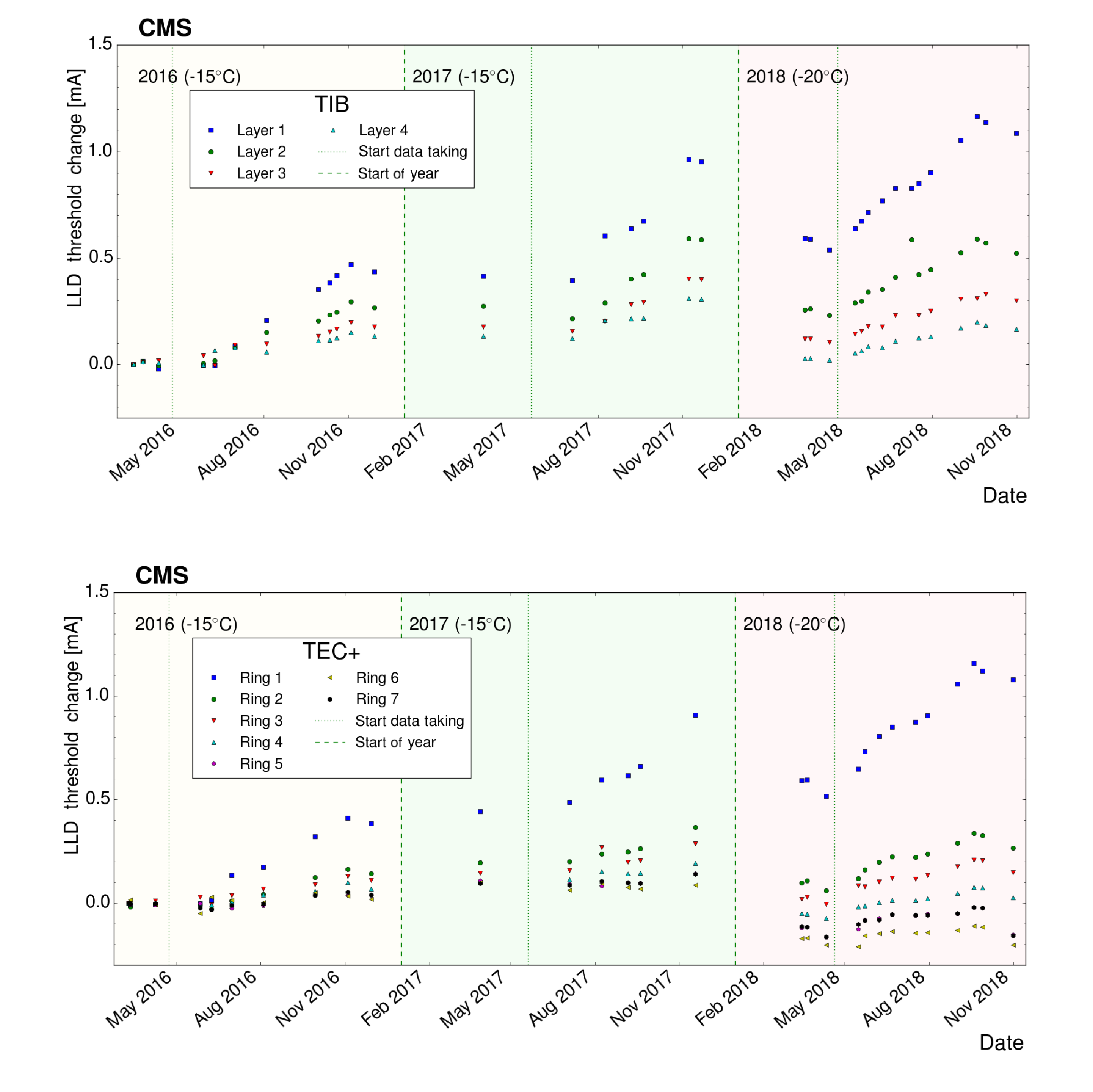
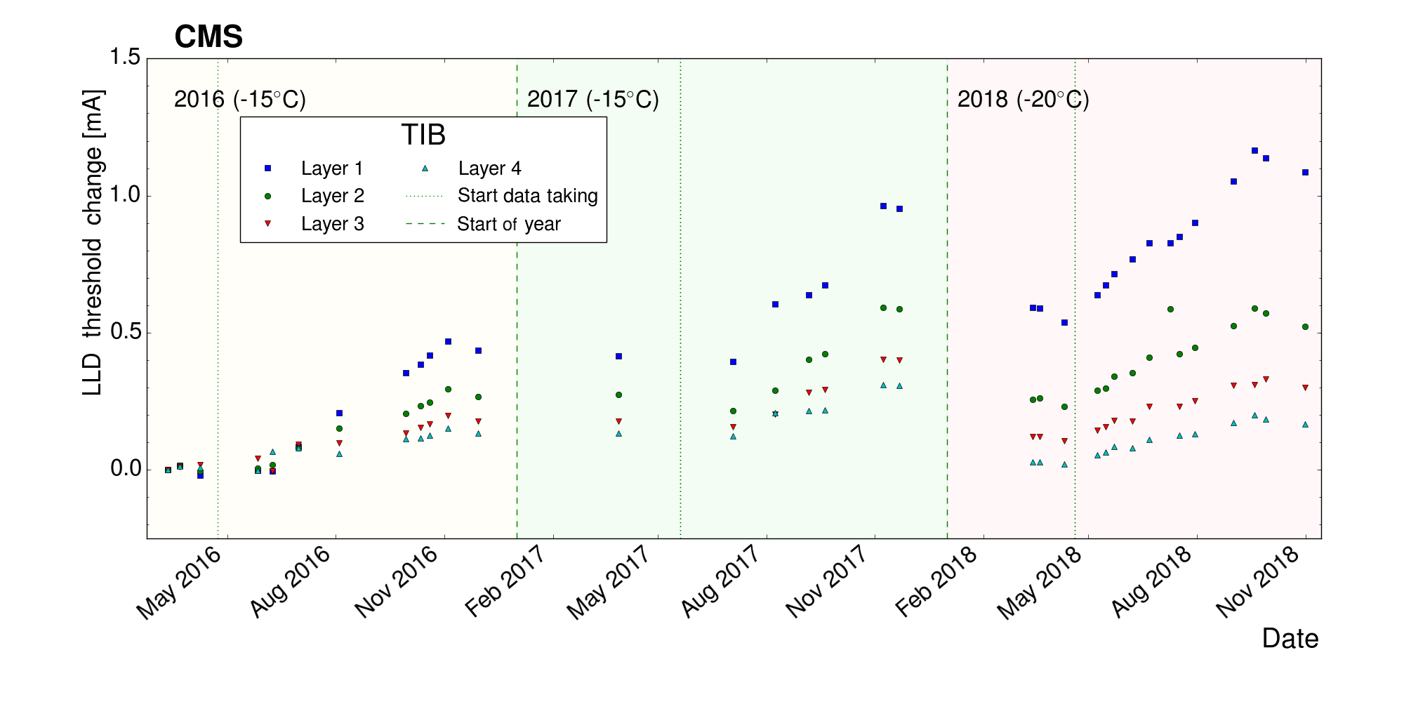
Figure 43:
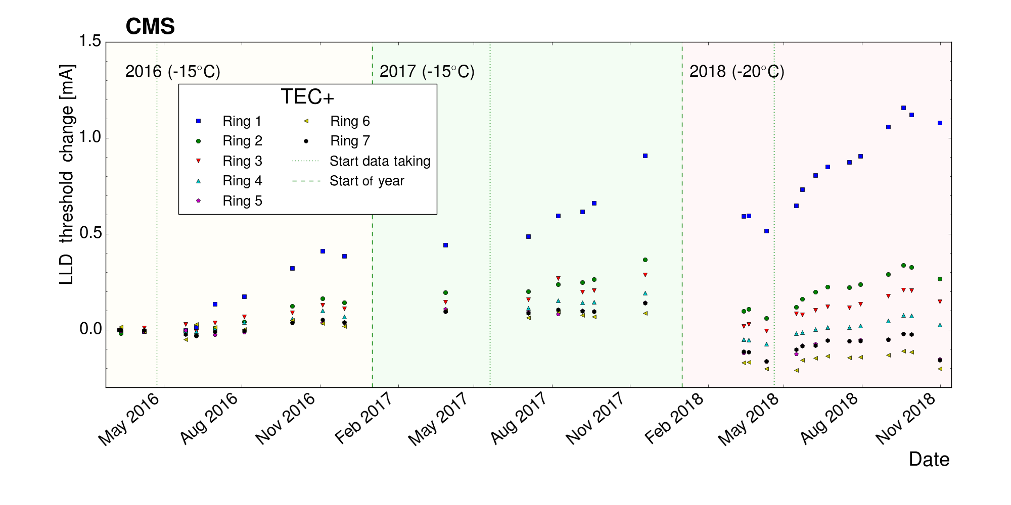
Laser driver threshold increase versus time for laser drivers in TIB (upper) and TEC$ + $ (lower). A point in early 2016, to which subsequent runs are compared, is defined for both readout partitions. |
png |
Figure 43-a:
Laser driver threshold increase versus time for laser drivers in TIB (upper) and TEC$ + $ (lower). A point in early 2016, to which subsequent runs are compared, is defined for both readout partitions. |
png |
Figure 43-b:
Laser driver threshold increase versus time for laser drivers in TIB (upper) and TEC$ + $ (lower). A point in early 2016, to which subsequent runs are compared, is defined for both readout partitions. |

png pdf |
Figure 44:
Thermal runaway observed in one power group of the TIB during the 2017 running. A power group consists of two high-voltage channels. The maximum high-voltage current of each channel is 12 mA. Once one of the two channels reaches this limit it is switched off (red dots). The modules connected to the other channel cool down as a result of this and the current decreases (blue squares). |
png pdf |
Figure 45:
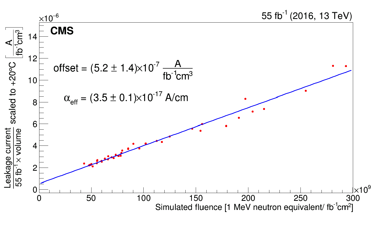
Leakage current per unit volume and integrated luminosity, scaled to $ +20^\circ $C, measured after an integrated luminosity of 55.4 fb$ ^{-1} $ as a function of the simulated fluence for modules at different radii. A linear fit to the data is performed and used to extract the effective current related damage rate, $ \alpha_{\text{eff}} $. |
png pdf |
Figure 46:
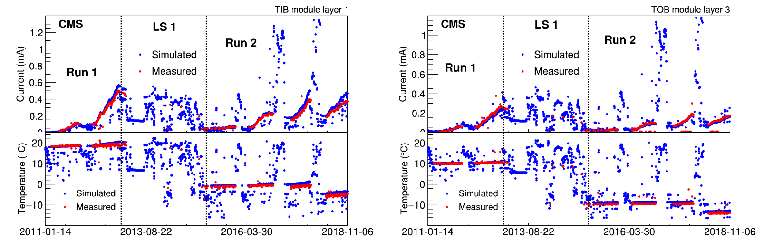
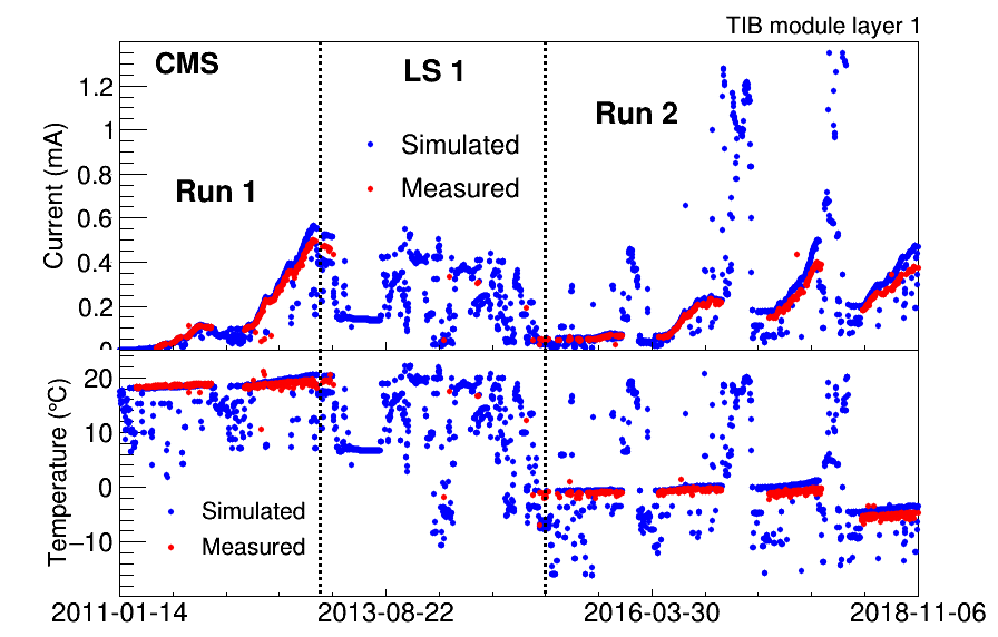
Leakage current and temperature measured by the DCU compared with simulation for a single module in the TIB layer 1 (left) and a module in TOB layer 3 (right). |
png |
Figure 46-a:
Leakage current and temperature measured by the DCU compared with simulation for a single module in the TIB layer 1 (left) and a module in TOB layer 3 (right). |
png |
Figure 46-b:
Leakage current and temperature measured by the DCU compared with simulation for a single module in the TIB layer 1 (left) and a module in TOB layer 3 (right). |
png pdf |
Figure 47:
Silicon temperature as measured by the DCUs of the individual modules after 192.3 fb$ ^{-1} $ of integrated luminosity, compared with simulation. |
png pdf |
Figure 48:
Left: leakage current as measured by the DCUs of the individual modules after 192.3 fb$ ^{-1} $ of integrated luminosity, compared with simulation. Right: relative difference between predicted and measured leakage current after 192.3 fb$ ^{-1} $. |
png |
Figure 48-a:
Left: leakage current as measured by the DCUs of the individual modules after 192.3 fb$ ^{-1} $ of integrated luminosity, compared with simulation. Right: relative difference between predicted and measured leakage current after 192.3 fb$ ^{-1} $. |
png |
Figure 48-b:
Left: leakage current as measured by the DCUs of the individual modules after 192.3 fb$ ^{-1} $ of integrated luminosity, compared with simulation. Right: relative difference between predicted and measured leakage current after 192.3 fb$ ^{-1} $. |
png pdf |
Figure 49:
Leakage current for each layer scaled to unit volume and 0$ ^\circ $C as a function of the total delivered integrated luminosity in the TIB (left) and TOB (right). The lower part of each plot shows the ratio of the measured and simulated current. |
png |
Figure 49-a:
Leakage current for each layer scaled to unit volume and 0$ ^\circ $C as a function of the total delivered integrated luminosity in the TIB (left) and TOB (right). The lower part of each plot shows the ratio of the measured and simulated current. |
png |
Figure 49-b:
Leakage current for each layer scaled to unit volume and 0$ ^\circ $C as a function of the total delivered integrated luminosity in the TIB (left) and TOB (right). The lower part of each plot shows the ratio of the measured and simulated current. |
png pdf |
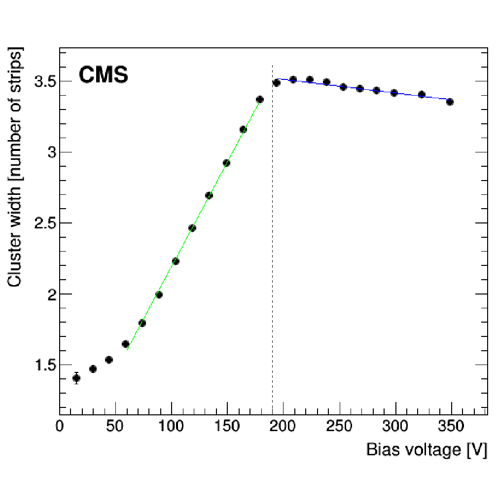
Figure 50:
Example of the determination of the full-depletion voltage using the intersection of two linear fits to the cluster size data of one module. The dashed line indicates the derived full-depletion voltage. |
png pdf |
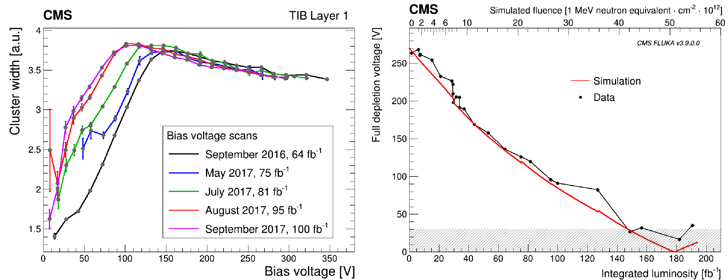
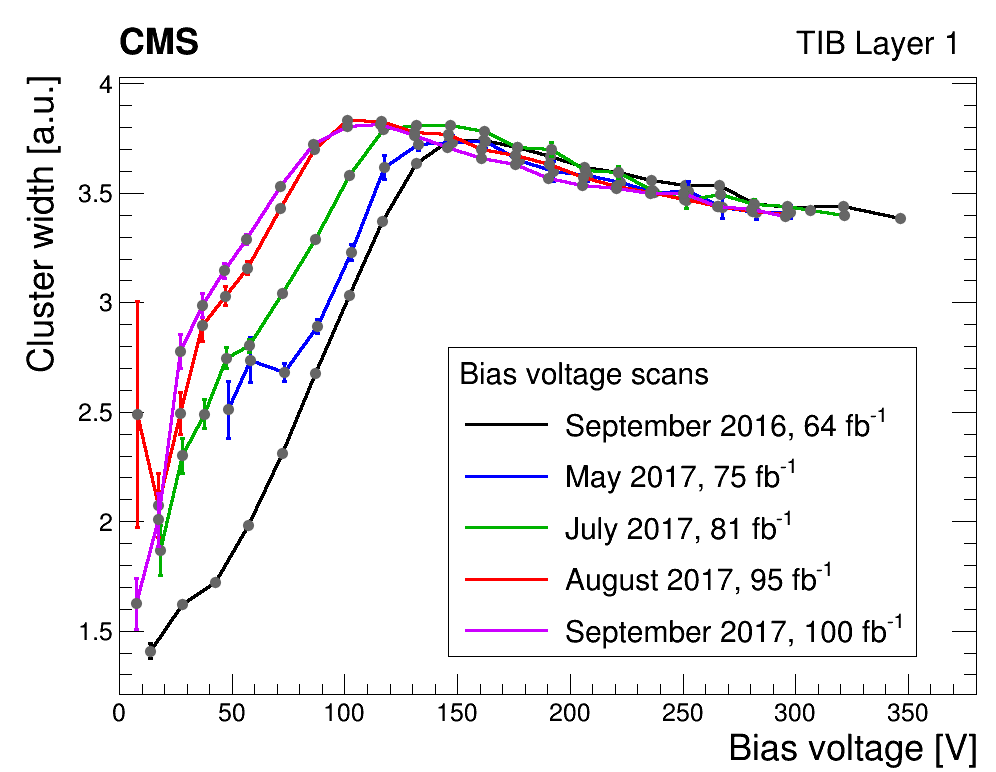
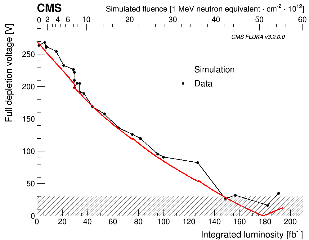
Figure 51:
Left: mean cluster width as a function of the sensor bias voltage for one module in the TIB layer 1 for bias scans taken at various integrated luminosities. The curves have been normalized to the same cluster width at the highest bias voltage of the scans. Right: evolution of the full-depletion voltage for one TIB layer 1 module as a function of the integrated luminosity (lower $ x $ axis) and fluence (upper $ x $ axis) using the data from bias scans. The red line shows the predicted full-depletion voltage. The gray hashed area indicates the region where depletion voltage estimates from data have a large uncertainty. |
png |
Figure 51-a:
Left: mean cluster width as a function of the sensor bias voltage for one module in the TIB layer 1 for bias scans taken at various integrated luminosities. The curves have been normalized to the same cluster width at the highest bias voltage of the scans. Right: evolution of the full-depletion voltage for one TIB layer 1 module as a function of the integrated luminosity (lower $ x $ axis) and fluence (upper $ x $ axis) using the data from bias scans. The red line shows the predicted full-depletion voltage. The gray hashed area indicates the region where depletion voltage estimates from data have a large uncertainty. |
png |
Figure 51-b:
Left: mean cluster width as a function of the sensor bias voltage for one module in the TIB layer 1 for bias scans taken at various integrated luminosities. The curves have been normalized to the same cluster width at the highest bias voltage of the scans. Right: evolution of the full-depletion voltage for one TIB layer 1 module as a function of the integrated luminosity (lower $ x $ axis) and fluence (upper $ x $ axis) using the data from bias scans. The red line shows the predicted full-depletion voltage. The gray hashed area indicates the region where depletion voltage estimates from data have a large uncertainty. |
png pdf |
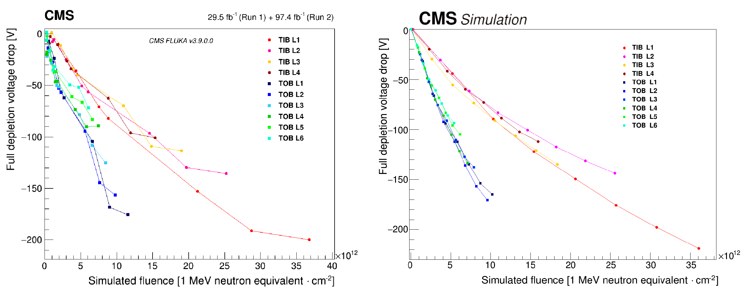
Figure 52:
Left: change of the full-depletion voltage in different tracker layers as a function of the particle fluence in data. Scans at different integrated luminosities are shown. The luminosity is converted to particle fluence for each position in the detector using a FLUKA model. Right: simulated change of the full-depletion voltage for single modules in different tracker layers as a function of the particle fluence. |
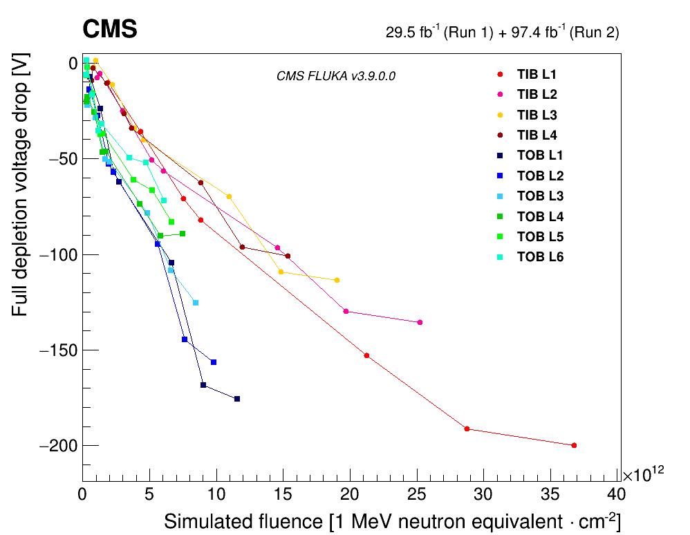
png |
Figure 52-a:
Left: change of the full-depletion voltage in different tracker layers as a function of the particle fluence in data. Scans at different integrated luminosities are shown. The luminosity is converted to particle fluence for each position in the detector using a FLUKA model. Right: simulated change of the full-depletion voltage for single modules in different tracker layers as a function of the particle fluence. |
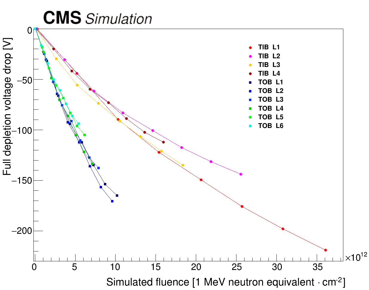
png |
Figure 52-b:
Left: change of the full-depletion voltage in different tracker layers as a function of the particle fluence in data. Scans at different integrated luminosities are shown. The luminosity is converted to particle fluence for each position in the detector using a FLUKA model. Right: simulated change of the full-depletion voltage for single modules in different tracker layers as a function of the particle fluence. |
png pdf |
Figure 53:
Tracker map of predicted leakage current at the end of life of the SST, where each silicon module is represented by a rectangle in the barrel and a trapezoid in the endcap; in stereo modules each submodule constitutes one half of this area. The color scale shows the projected sensor leakage current for a total integrated luminosity of 500 fb$ ^{-1} $ with the SST operated at $ -25^{\circ} $C during all of Run 3. Modules in dark gray were already inoperable at the end of Run 2. Modules in light gray are expected to become inoperable during Run 3 because their projected leakage current will be too high. Regions in purple are control rings with DCU readout issues, implying no input data for the simulation. |
png pdf |
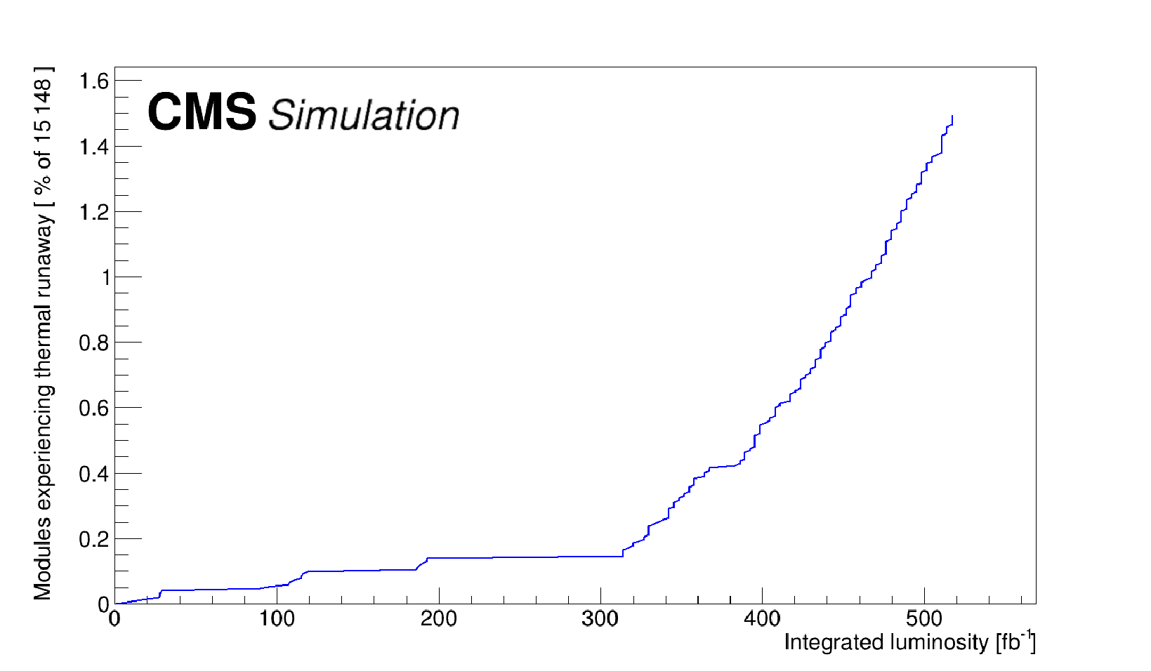
Figure 54:
Fraction of modules affected by thermal runaway as a function of the integrated luminosity. |
png pdf |
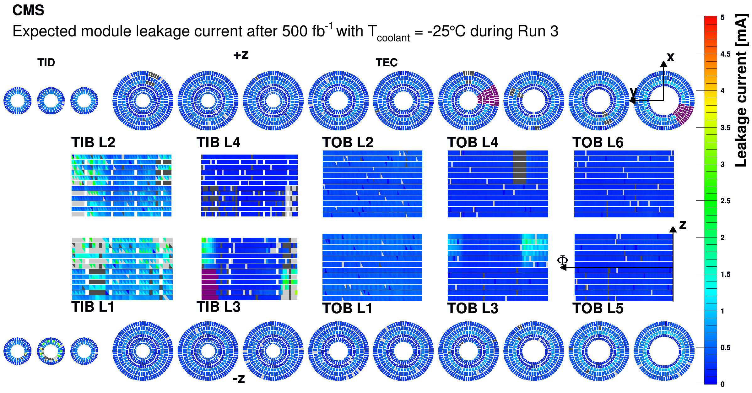
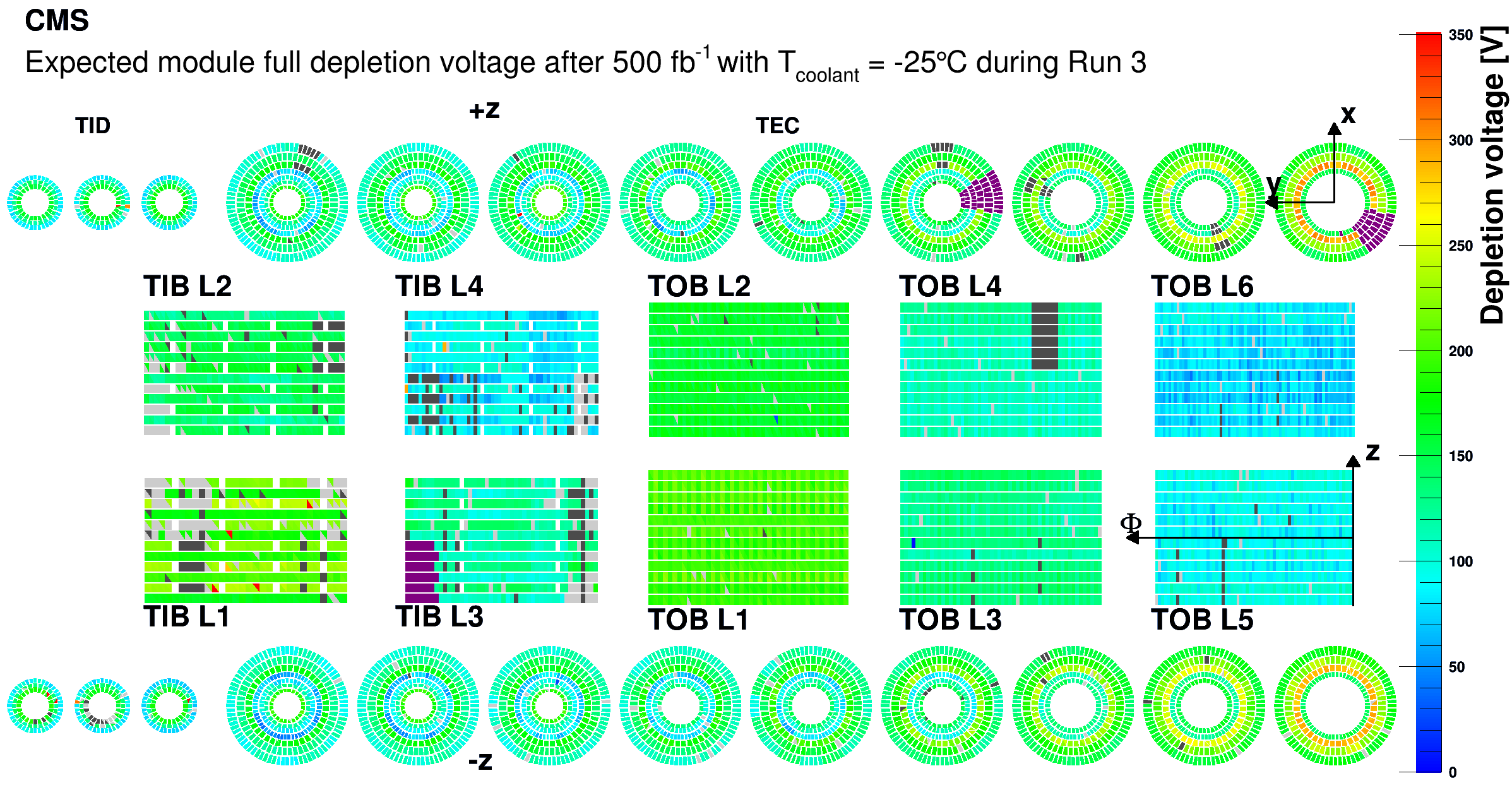
Figure 55:
Tracker map of predicted full-depletion voltage at the end of life of the SST, where each silicon module is represented by a rectangle in the barrel and a trapezoid in the endcap; in stereo modules each submodule constitutes one half of this area. The color scale shows the projected full-depletion voltage for a total integrated luminosity of 500 fb$ ^{-1} $ with the SST operated at $ -25^{\circ} $C during all of Run 3. Modules in dark gray were already inoperable at the end of Run 2. Modules in light gray are expected to become inoperable during Run 3 because their projected leakage current will be too high and are identical to the modules depicted in light grey in Fig. 53. Regions in purple are control rings with DCU readout issues, implying no input data for the simulation. |
| Tables | |
png pdf |
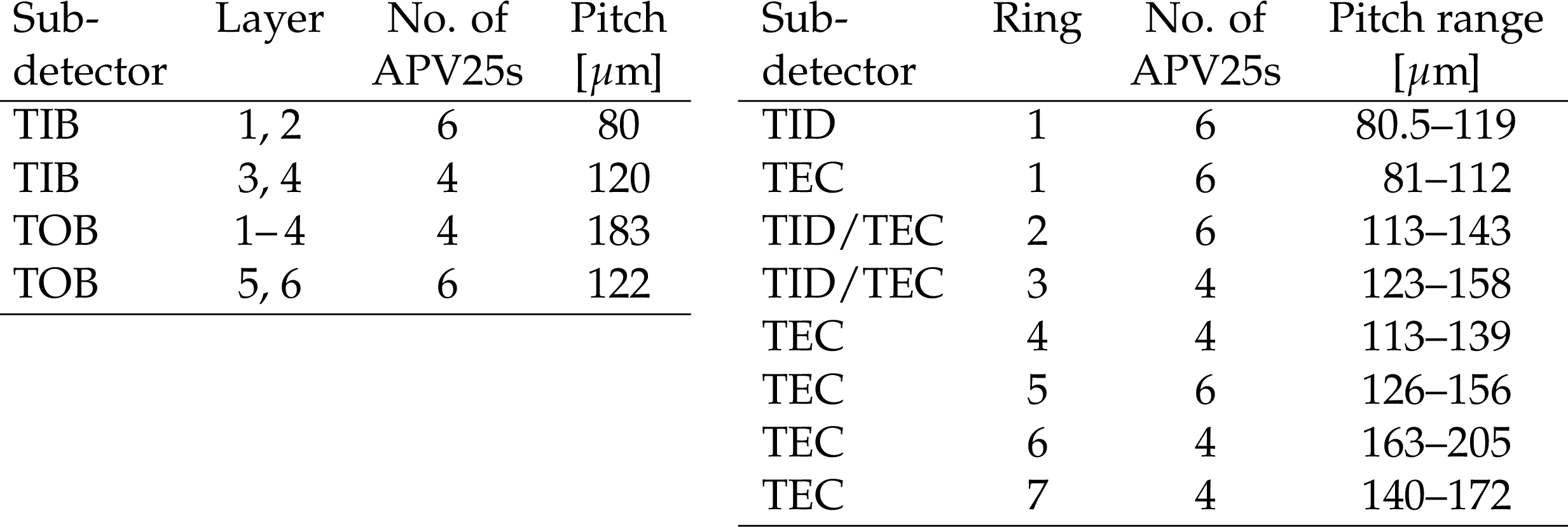
Table 1:
Summary of number of APV25 chips per module and strip pitch (strip pitch range) for barrel (endcap) sensor geometries. |
png pdf |
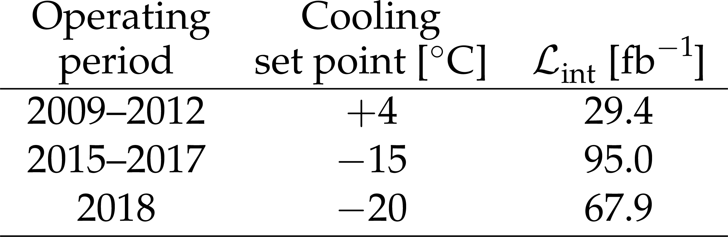
Table 2:
Cooling plant set points of the SST during different operating periods and integrated luminosity acquired during each period. |
png pdf |
Table 3:
Simulated and measured weights of the SST and of three of its partitions. |
png pdf |
Table 4:
Cross talk measured in the barrel in 2018, obtained with cosmic ray data taken without magnetic field. Results are summarized as the average fraction $ f_0 $ of observed charge for the leading strip, the fraction $ f_1 $ on each of the two neighboring strips, and the fraction $ f_2 $ on each of the strips next to these neighboring strips. |
png pdf |
Table 5:
Fraction of live channels in the different readout partitions of the SST at the end of data taking in 2018. |
| Summary |
| References | ||||
| 1 | CMS Collaboration | The CMS experiment at the CERN LHC | JINST 3 (2008) S08004 | |
| 2 | L. Evans and P. Bryant (editors) | LHC machine | JINST 3 (2008) S08001 | |
| 3 | CMS Collaboration | The CMS tracker system project: Technical Design Report | Technical design report CERN-LHCC-98-06, CMS-TDR-5,, \urlhttps://cds.cern.ch/record/368412, 1997 CDS |
|
| 4 | Tracker Group of the CMS Collaboration | CMS Technical Design Report for the pixel detector upgrade | CMS Technical Design Report CERN-LHCC-2012-016, CMS-TDR-11, 2012 | |
| 5 | Tracker Group of the CMS Collaboration | The CMS Phase-1 pixel detector upgrade | JINST 16 (2021) P02027 | 2012.14304 |
| 6 | CMS Collaboration | The CMS tracker: addendum to the Technical Design Report | Tech. Design Report CERN-LHCC-2000-016, CMS-TDR-5-add-1, 2000 CDS |
|
| 7 | Tracker Group of the CMS Collaboration | Track reconstruction with cosmic ray data at the tracker integration facility | CMS Note CMS-NOTE-2009-003, 2008 | |
| 8 | Tracker Group of the CMS Collaboration | Performance studies of the CMS strip tracker before installation | JINST 4 (2009) P06009 | 0901.4316 |
| 9 | CMS Collaboration | Commissioning and performance of the CMS silicon strip tracker with cosmic ray muons | JINST 5 (2010) T03008 | CMS-CFT-09-002 0911.4996 |
| 10 | CMSnoop | Public CMS luminosity information | \hrefCMS Collaboration, \urlhttps://twiki.cern.ch/twiki/bin/view/CMSPublic/LumiPublicResults. accessed on April 5, 2019 | |
| 11 | CMS Collaboration | Description and performance of track and primary-vertex reconstruction with the CMS tracker | JINST 9 (2014) P10009 | CMS-TRK-11-001 1405.6569 |
| 12 | CMS Collaboration | Development of the CMS detector for the CERN LHC Run 3 | JINST 19 (2024) P05064 | CMS-PRF-21-001 2309.05466 |
| 13 | L. L. Jones et al. | The APV25 deep submicron readout chip for CMS detectors | Fifth workshop on electronics for LHC experiments, Snowmass, USA, 20-24 September 199 (1900) 9 |
|
| 14 | G. Cervelli , A. Marchioro , P. Moreira , and F. Vasey | A linear laser-driver array for optical transmission in the LHC experiments | in IEEE Nuclear Science Symposium, volume 2, 2000 link |
|
| 15 | J. Troska et al. | Optical readout and control systems for the CMS tracker | IEEE Trans. Nucl. Sci. 50 (2003) 1067 | |
| 16 | J. A. Coughlan et al. | The CMS tracker front-end driver | 9th Workshop on electronics for LHC experiments, Amsterdam, Netherlands, 29 September-3 October 200 (1900) 3 |
|
| 17 | C. Paillard, C. Ljuslin, and A. Marchioro | The CCU25: a network oriented communication and control unit integrated circuit in a 0.25$ \mu\text{m} $ CMOS technology | 8th Workshop on electronics for LHC experiments, Colmar, France, 9-13 September 200 (1900) 2 |
|
| 18 | K. A. Gill et al. | Progress on the CMS tracker control system | 11th Workshop on Electronics for LHC and Future Experiments, Heidelberg, Germany, 12-16 September 200 (1900) 5 |
|
| 19 | L. Borrello, A. Messineo, E. Focardi, and A. Macchiolo | Sensor design for the CMS silicon strip tracker | Technical Report CMS-NOTE-2003-020, 2003 | |
| 20 | S. Braibant et al. | Investigation of design parameters for radiation hard silicon microstrip detectors | NIM A 485 (2002) 343 | |
| 21 | S. Gadomski et al. | The deconvolution method of fast pulse shaping at hadron colliders | NIM A 320 (1992) 217 | |
| 22 | G. Magazzu, A. Marchioro, and P. Moreira | The detector control unit: an ASIC for the monitoring of the CMS silicon tracker | IEEE Trans. Nucl. Sci. 51 (2004) 1333 | |
| 23 | P. Placidi, A. Marchioro, P. Moreira, and K. C. Kloukinas | A 40 MHz clock and trigger recovery circuit for the CMS tracker fabricated in a 0.25\unit$ \mu\text{m} $ CMOS technology and using a self calibration technique | Fifth workshop on electronics for LHC experiments, Snowmass, USA, 20-24 September 199 (1900) 9 |
|
| 24 | CMSnoop | I$ ^2 $C-bus specification and user manual | \hrefNXP, \urlhttps://www.nxp.com/docs/en/user-guide/UM4.pdf, 1020 | |
| 25 | S. Paoletti, A. Bocci, R. D'Alessandro, and G. Parrini | The powering scheme of the CMS tracker | 10th workshop on electronics for LHC and future experiments, Boston, USA, 13-17 September 200 (1900) 4 |
|
| 26 | CMS Collaboration | Commissioning the CMS silicon strip tracker prior to operations with cosmic ray muons | CMS Note CMS-NOTE-2009-021, 2009 CDS |
|
| 27 | S. Dris, K. Gill, J. Troska, and F. Vasey | Predicting the gain spread of the CMS tracker analog readout optical links | CMS Note CMS-NOTE-2006-145, 2006 | |
| 28 | C. Delaere and L. Mirabito | Timing of the CMS tracker: Study of module properties | CMS NOTE CMS-NOTE-2007-027, 2007 | |
| 29 | CMS Collaboration | CMS full simulation for Run-2 | J. Phys. Conf. Ser. 664 (2015) 072022 | |
| 30 | GEANT4 Collaboration | GEANT 4---a simulation toolkit | NIM A 506 (2003) 250 | |
| 31 | M. Jansova | Recherche du partenaire supersymétrique du quark top et mesure des propriétés des dépots dans le trajectographe \`a pistes de silicium de l'expérience CMS au Run 2 | PhD thesis, Université de Strasbourg,, \urlhttps://cds.cern.ch/record/2647308/, 2018 link |
|
| 32 | CMS Collaboration | Strategies and performance of the CMS silicon tracker alignment during LHC Run 2 | NIM A 1037 (2022) 166795 | CMS-TRK-20-001 2111.08757 |
| 33 | Particle Data Group , S. Navas et al. | Review of particle physics | PRD 110 (2024) 030001 | |
| 34 | C. Foudas et al. | The CMS tracker readout front end driver | IEEE Trans. Nucl. Sci. 52 (2005) 2836 | |
| 35 | CMS Collaboration | Measurements of inclusive $ W $ and $ Z $ cross sections in $ pp $ collisions at $ \sqrt{s}= $ 7 TeV | JHEP 01 (2011) | CMS-EWK-10-002 1012.2466 |
| 36 | CMS Collaboration | Muon tracking performance in the CMS Run 2 legacy data using the tag-and-probe technique | CMS DP CMS-DP-2020-035, 2020 CDS |
|
| 37 | L. Tuura, A. Meyer, I. Segoni, and G. D. Ricca | CMS data quality monitoring: Systems and experiences | J. Phys. Conf. Ser. 219 (2010) 072020 | |
| 38 | L. Quertenmont | Search for heavy stable charged particles with the CMS detector at the LHC | PhD thesis, Université catholique de Louvain, 2010 link |
|
| 39 | V. Bartsch et al. | An algorithm for calculating the Lorentz angle in silicon detectors | NIM A 497 (2003) 389 | physics/0204078 |
| 40 | W. Adam et al. | The effect of highly ionising particles on the CMS silicon strip tracker | NIM A 543 (2005) 463 | |
| 41 | et al. | The effect of highly ionising events on the APV25 readout chip | R. Bainbridge CMS Note CMS-NOTE-2002-038, 2002 link |
|
| 42 | CMS Tracker Collaboration | Stand-alone cosmic muon reconstruction before installation of the CMS silicon strip tracker | JINST 4 (2009) P05004 | 0902.1860 |
| 43 | P. Aarnio, K. Ekman, T. Nyman, and P. Salonen | CMS, the Compact Muon Solenoid: Technical Proposal | LHC tech. proposal CERN/-38, LHCC/P1, 1994 LHCC 9 (1994) 4 |
|
| 44 | CMS Collaboration | Search for long-lived charged particles in proton-proton collisions at $ \sqrt{s}= $ 13 TeV | PRD 94 (2016) 112004 | CMS-EXO-15-010 1609.08382 |
| 45 | M. Moll | Radiation damage in silicon particle detectors: Microscopic defects and macroscopic properties | PhD thesis, Hamburg University, 1999 link |
|
| 46 | K. Gill et al. | Radiation hardness assurance and reliability testing of InGaAs photodiodes for optical control links for the CMS experiment | IEEE Trans. Nucl. Sci. 52 (2005) 1480 | |
| 47 | A. Ferrari, P. R. Sala, A. Fass \`o , and R. Johannes | FLUKA: A multi-particle transport code (program version 2005) | link | |
| 48 | T. T. Bohlen et al. | The FLUKA code: developments and challenges for high energy and medical applications | Nucl. Data Sheets 120 (2014) 211 | |
| 49 | Thresh | Laser threshold current and efficiency at temperatures between $ -20^{\circ} $C and $ +20^{\circ} $C | \href https://edms.cern.ch/ui/file/430290/1/-Eff-Temp.pdfR. Macias,, EDMS document, CMS-TK-TR-0036, \url https://edms.cern.ch/ui/file/430290/1/Thresh-Eff-Temp.pdf, 2003 | |
| 50 | K. A. Gill, R. Grabit, J. K. Troska, and F. Vasey | Radiation hardness qualification of InGaAsP/InP 1310-nm lasers for the CMS tracker optical links | IEEE Trans. Nucl. Sci. 49 (2002) 2923 | |
| 51 | T. Kohriki et al. | First observation of thermal runaway in the radiation damaged silicon detector | IEEE Trans. Nucl. Sci. 43 (1996) 1200 | |
|
|
Compact Muon Solenoid LHC, CERN |
|
|
|
|
|
|